System for reducing row periphery power consumption in memory devices

a memory device and row periphery technology, applied in the field of semiconductor devices, can solve the problems of inability to fully or even partially power down the circuitry surrounding a given row (i.e., the row-periphery circuitry) and the stability and integrity of the data stored in the corresponding row, and achieve the effect of reducing the power consumption of the row periphery, reducing the operating voltage and power consumption, and avoiding negative effects on the stability and reliability of data stored

Active Publication Date: 2005-02-17
TEXAS INSTR INC
View PDF3 Cites 3 Cited by
  • Summary
  • Abstract
  • Description
  • Claims
  • Application Information

AI Technical Summary

Benefits of technology

[0008] The present invention provides a versatile system for reducing row periphery power consumption in memory devices—particularly SRAM devices—in an easy, efficient and cost-effective manner. The present invention provides apparatus and methods for powering down row-periphery circuitry without negatively impacting the stability and reliability of data stored in a corresponding wordline. Specifically, the present invention provides intervention, or keeper, circuitry instantiated on, or in immediate proximity to, a given wordline. Prior to sleep mode, the intervention circuitry is activated, holding that wordline at its non-accessed state. Wordline driver circuitry, and other circuitry preceding the intervention circuitry (hereafter generally referred to as control circuitry), is then safely powered down without impacting the integrity of the row data. The present invention thus provides optimal power savings in sleep mode while overcoming limitations associated with conventional memory designs.
[0009] More specifically, the present invention provides a method of reducing power consumption in a semiconductor memory device having a row of memory cells and circuitry for operating the row of memory cells. The method comprises providing an intervention circuit, and instantiating the intervention circuit within the circuitry for operating the row of memory cells, proximal to the row of memory cells. The intervention circuit is operated to retain the row of memory cells in a desired state, and the circuitry for operating the row of memory cells preceding the intervention circuit is powered down.

Problems solved by technology

Often, circuitry surrounding a given row (i.e., the row-periphery circuitry) cannot be fully, or even partially, powered down.
If this row-periphery circuitry is powered down, the stability and integrity of the data stored in a corresponding row is adversely affected.
Furthermore, considerable efforts have been made to reduce the geometry and feature sizes, and thus the operating voltages and power consumption, of almost all semiconductor fabrication technologies.
Transistors and other structures fabricated in smaller device technologies generally become more susceptible to leakage current problems.
Thus, the movement to smaller device technologies has increased, particularly in SRAM designs, the prevalence and importance of leakage current considerations and problems.
Where, however, row-periphery circuitry is not, or cannot, be powered down, leakage currents through the row-periphery become, relative to leakage currents of surrounding array circuitry, extremely large.
This reduces the power savings realized during sleep mode.

Method used


Image

  • System for reducing row periphery power consumption in memory devices
  • System for reducing row periphery power consumption in memory devices
  • System for reducing row periphery power consumption in memory devices

Examples


Embodiment Construction

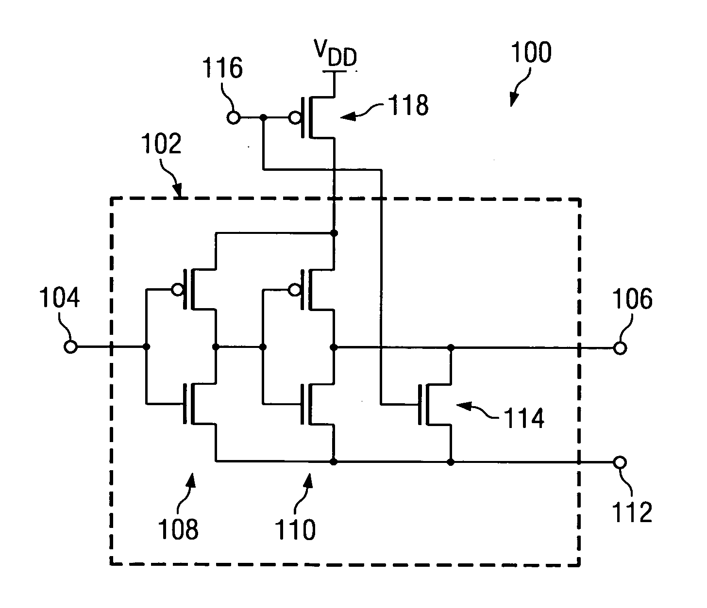
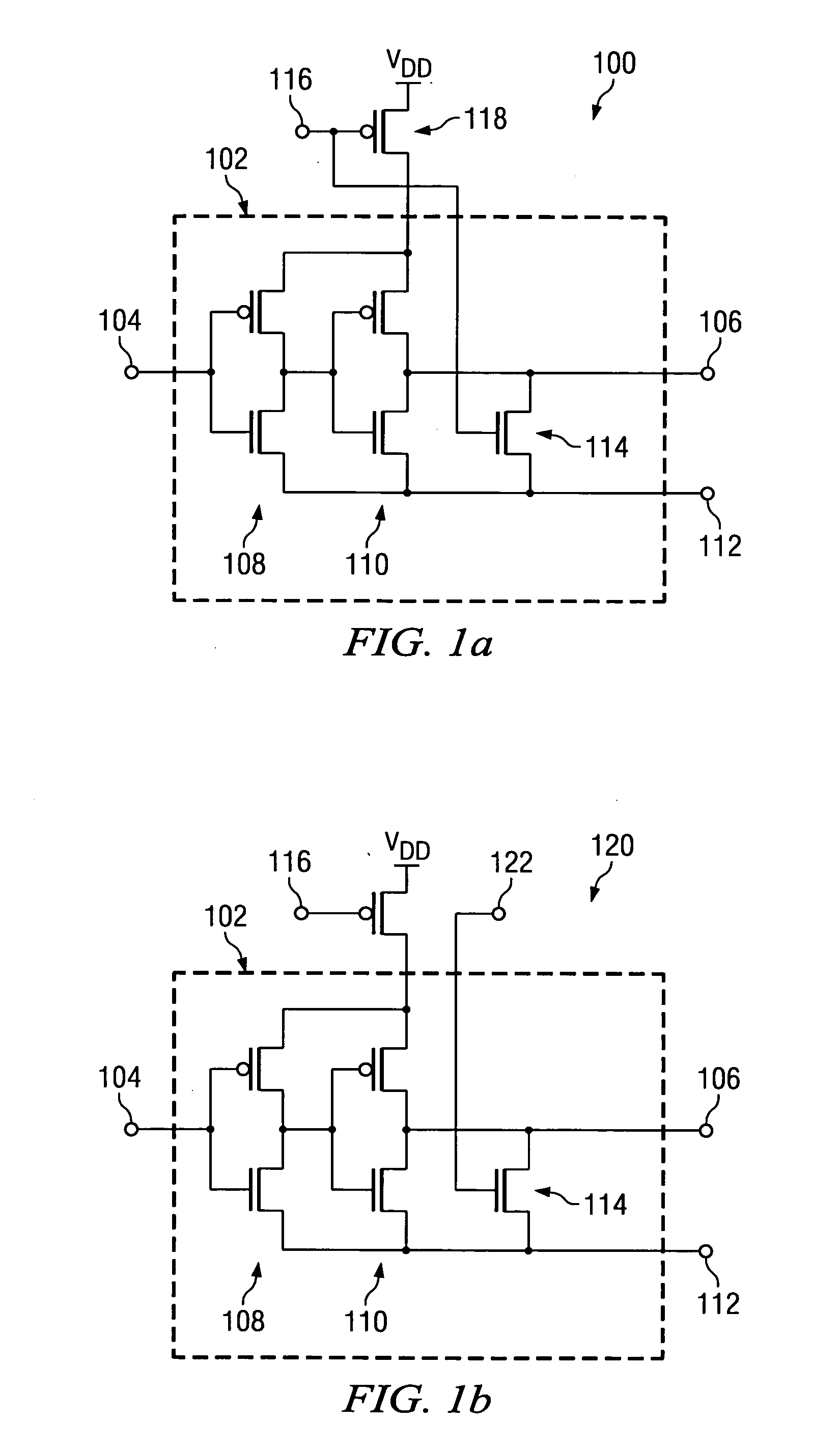
[0019] While the making and using of various embodiments of the present invention are discussed in detail below, it should be appreciated that the present invention provides many applicable inventive concepts, which can be embodied in a wide variety of specific contexts. The invention will now be described in conjunction with SRAM memory architecture. The specific embodiments discussed herein are merely illustrative of specific ways to make and use the invention and do not limit the scope of the invention.

[0020] The present invention provides a versatile system that reduces SRAM power consumption during sleep mode. As previously noted, minimizing SRAM standby power during sleep mode is critical to many power sensitive applications, especially those that rely on low-voltage battery sources for power (e.g., wireless communications devices).

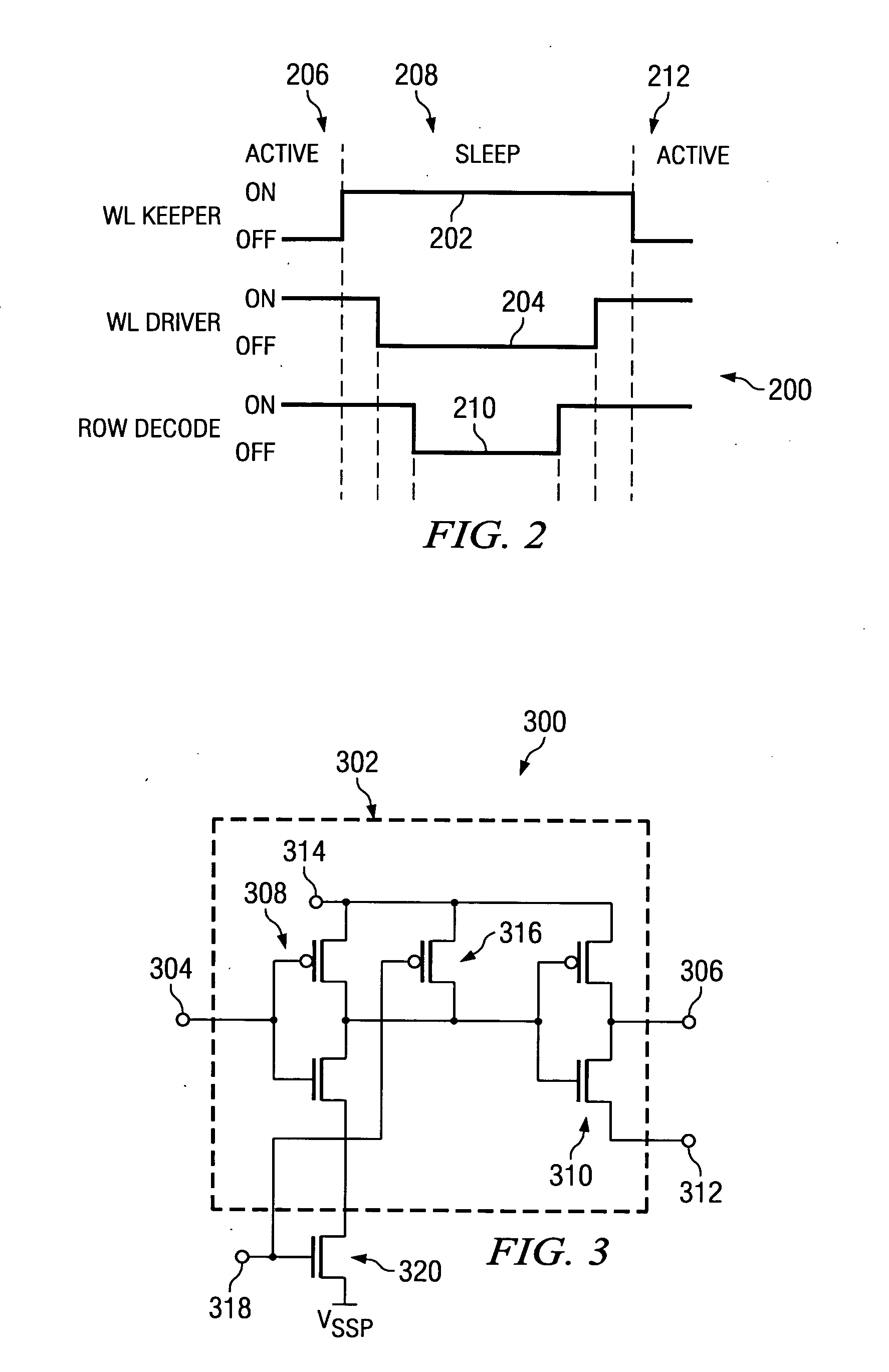
[0021] For an array during sleep mode, conventional systems often relied on raising ground voltage levels, with respect to supply voltage levels,...


PUM


Abstract

The present invention provides a system for reducing row periphery power consumption in a semiconductor memory device, particularly during sleep mode operation. A memory device (100) according to the present invention has a row (106) of memory cells and driver circuitry (102) preceding the row of memory cells. The present invention provides an intervention circuit (114) instantiated within the driver circuitry proximal to the row of memory cells. The intervention circuit is operated to hold the row of memory cells at a desired state, while the driver circuitry (108, 110) preceding the intervention circuit is powered down.

Description

TECHNICAL FIELD OF THE INVENTION [0001] The present invention relates generally to the field of semiconductor devices and, more particularly, to a system for reducing row periphery power consumption in memory devices. BACKGROUND OF THE INVENTION [0002] Memory systems are known in the art and used in nearly all microprocessor and digital equipment applications. Memory systems generally utilize different types of memory for different applications. One such type of memory is Static Random Access Memory (“SRAM”). SRAM systems have the advantage of high speed and ease of use as compared to some other types of memory systems. In addition, SRAM systems using MOS technology exhibit extremely low standby power and do not require a refresh cycle to maintain the information stored in the SRAM system. These attributes make SRAM systems particularly desirable for portable equipment, such as laptop computers. As a result, SRAM arrays are becoming an increasingly large portion of many integrated c...

Claims


Application Information

Patent Timeline
Patent Type & Authority Applications(United States)
IPC IPC(8): G11C8/08G11C11/417
CPCG11C11/417G11C8/08
Inventor DENG, XIAOWEIHOUSTON, THEODORE W.SHEFFIELD, BRYAN D.
Owner TEXAS INSTR INC
Why Eureka
Try Eureka