Robot blade for handling of semiconductor waffers

a robotic blade and semiconductor technology, applied in the field of semiconductor wafer processing, can solve the problems of delamination of wafers and save considerable time and money, and achieve the effect of preventing delamination or peeling of the distal end, reducing the risk of delamination and avoiding the deterioration of any portion

Inactive Publication Date: 2005-02-17
TEXAS INSTR INC
View PDF17 Cites 3 Cited by
  • Summary
  • Abstract
  • Description
  • Claims
  • Application Information

AI Technical Summary

Benefits of technology

[0005] Embodiments of the invention provide a number of technical advantages. Embodiments of the invention may include all, some, or none of these advantages. In one embodiment, a robot blade utilized for transferring semiconductor wafers in a transfer chamber includes rounded edges at its distal end that eliminates deterioration of any portion of the distal end due to thermal cycling or other factors. This assures that no particles associated with the robot blade material get embedded in the semiconductor wafer that the robot blade is handling or fall onto a lower semiconductor wafer, which may cause defective wafers. In addition, wafer breakage may be avoided by preventing any delamination or peeling of the distal end of the robot blade. Reducing defects in, or breakage of, semiconductor wafers during their handling greatly improves yield, which saves considerable time and money.

Problems solved by technology

This assures that no particles associated with the robot blade material get embedded in the semiconductor wafer that the robot blade is handling or fall onto a lower semiconductor wafer, which may cause defective wafers.
Reducing defects in, or breakage of, semiconductor wafers during their handling greatly improves yield, which saves considerable time and money.

Method used


Image

  • Robot blade for handling of semiconductor waffers
  • Robot blade for handling of semiconductor waffers

Examples


Embodiment Construction

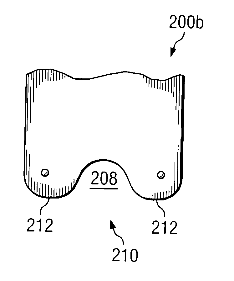
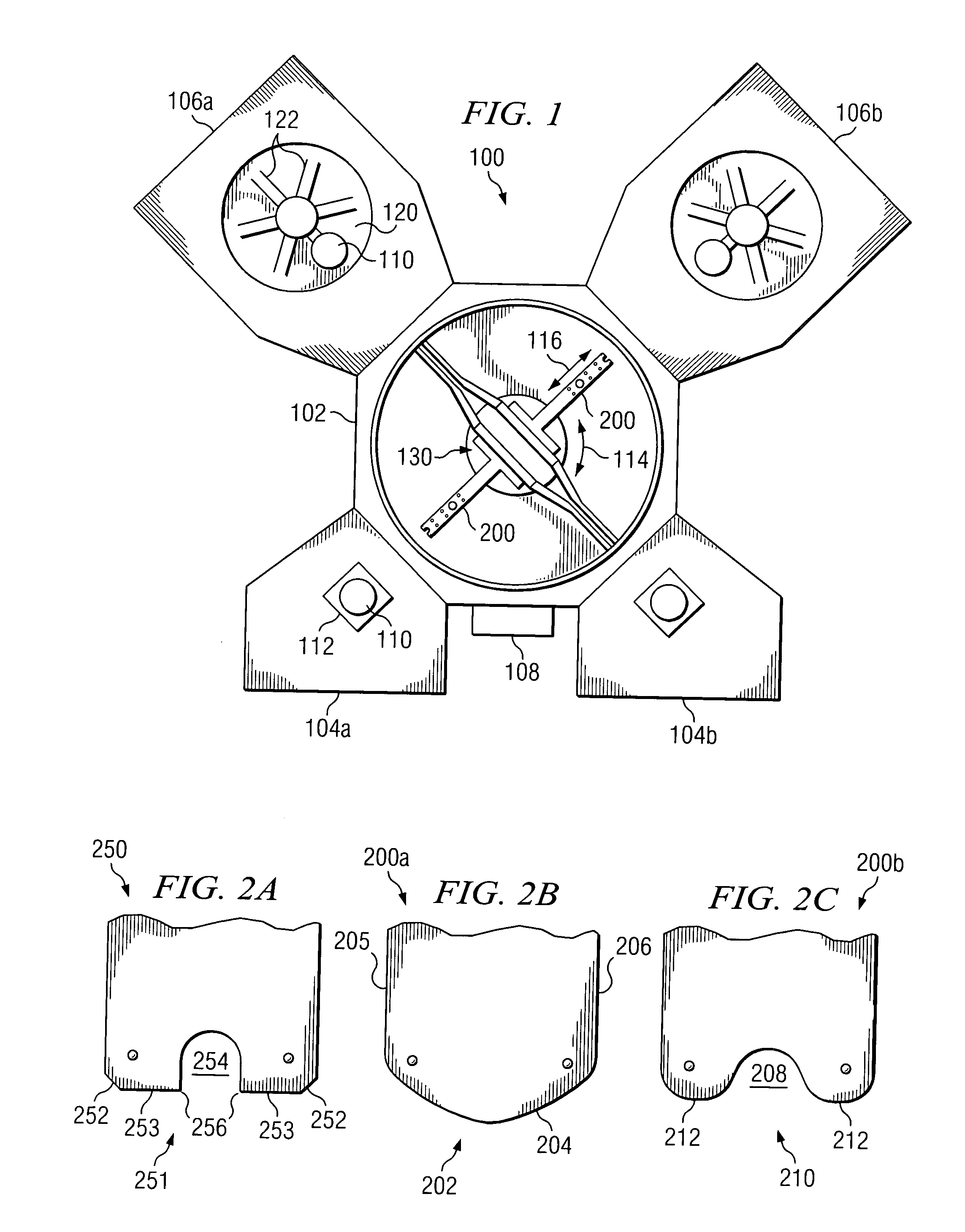
[0012] Example embodiments of the present invention and their advantages are best understood by referring now to FIGS. 1 and 2C of the drawings, in which like numerals refer to like parts.

[0013]FIG. 1 is a partial plan view of a wafer processing system 100 in accordance with one embodiment of the present invention. Processing system 100 generally represents the SEQUEL family of processing systems manufactured by Novellus Systems, Inc.; however, other suitable processing systems are contemplated by the present invention. In the illustrated embodiment, processing system 100 includes a transfer chamber 102 disposed between a pair of load locks 104a, 104b and a pair of process chambers 106a, 106b. Processing system 100 also includes a cool station 108.

[0014] Transfer chamber 102 includes a pair of robot blades 200 (also known as end effectors) that function to transfer semiconductor wafers 110 or other suitable substrates within processing system 100. Accordingly, robot blades 200 are...


PUM


Abstract

According to one embodiment of the invention, a system for handling semiconductor wafers includes a chamber, a robot associated with the chamber, and a robot blade generally horizontally disposed within the chamber and coupled to the robot at a first end. The robot blade includes a second end distal the first end, in which the second end has a plan view profile that forms a continuously curved surface.

Description

TECHNICAL FIELD OF THE INVENTION [0001] The present invention relates generally to semiconductor wafer processing and, more particularly, to a robot blade for handling of semiconductor wafers. BACKGROUND OF THE INVENTION [0002] Semiconductor wafers are subjected to many different processes in order to manufacture semiconductor die on the wafer. Semiconductor wafers are typically transferred between processing chambers in order to carry out the different processes. For efficiency purposes, a robot is used to transfer the wafers between chambers. A robot blade associated with the robot, sometimes referred to as an end effector, is used to transfer individual wafers. Depending on the process chamber that the robot blade is transferring the semiconductor wafer to, the robot blade may see temperature fluctuations. [0003] Current robot blades have distal ends (the ends that are proximate the semiconductor wafers during transferring) that have straight edges that result in sharp corners (a...

Claims


Application Information

Patent Timeline
Patent Type & Authority Applications(United States)
IPC IPC(8): H01L21/677B65G49/07H01L21/68
CPCH01L21/67742
Inventor GARCIA, MARTIN
Owner TEXAS INSTR INC
Why Eureka
Try Eureka