Method and apparatus for manufacturing semiconductor

a technology of semiconductors and manufacturing methods, applied in the direction of photomechanical equipment, instruments, printers, etc., can solve the problems of excessively large or small masking blades, non-uniformity generation, and defect developmen

Inactive Publication Date: 2005-02-17
OLYMPUS CORP
View PDF11 Cites 49 Cited by
  • Summary
  • Abstract
  • Description
  • Claims
  • Application Information

AI Technical Summary

Benefits of technology

[0035]FIG. 12 is a diagram showing detected places of the edge rinsed cut width in the ap

Problems solved by technology

However, in the coater in the photolithography device, non-uniformity is generated in forming the film of the photoresist 3 onto the surface of the semiconductor wafer 1 by attached foreign matters, photoresist viscosity, and rotation conditions.
A masking blade is excessively large or small.
In the developer, a developing de

Method used


Image

  • Method and apparatus for manufacturing semiconductor
  • Method and apparatus for manufacturing semiconductor
  • Method and apparatus for manufacturing semiconductor

Examples


first embodiment

[0051] the present invention will be described hereinafter with reference to the drawings.

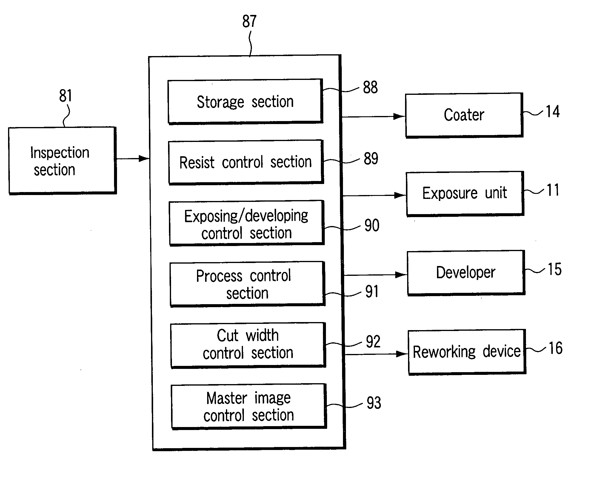
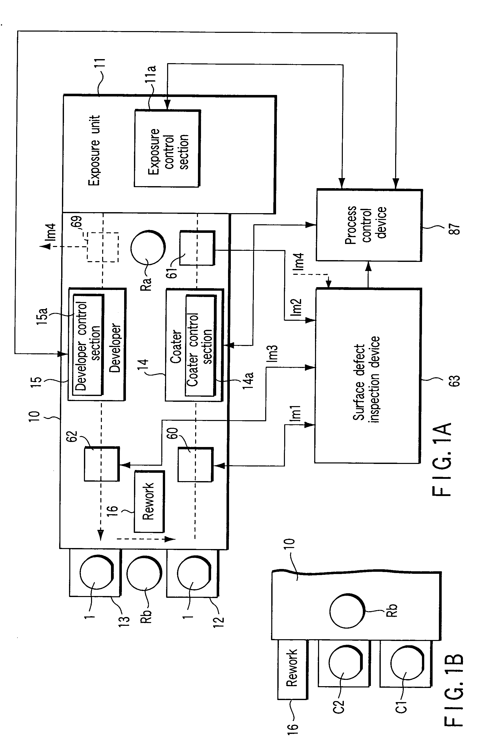
[0052]FIG. 1A is a constitution diagram of a semiconductor manufacturing apparatus disposed in a photolithography step. The semiconductor manufacturing apparatus includes a coater / developer 10 and an exposure unit 11. A cassette 12 is disposed in a throw-in port of the coater / developer 10. The cassette 12 stores a plurality of semiconductor wafers 1 before a photolithography process. A cassette 13 is disposed in a take-out port of the coater / developer 10. The cassette 13 stores the plurality of semiconductor wafers 1 subjected to the photolithography process.

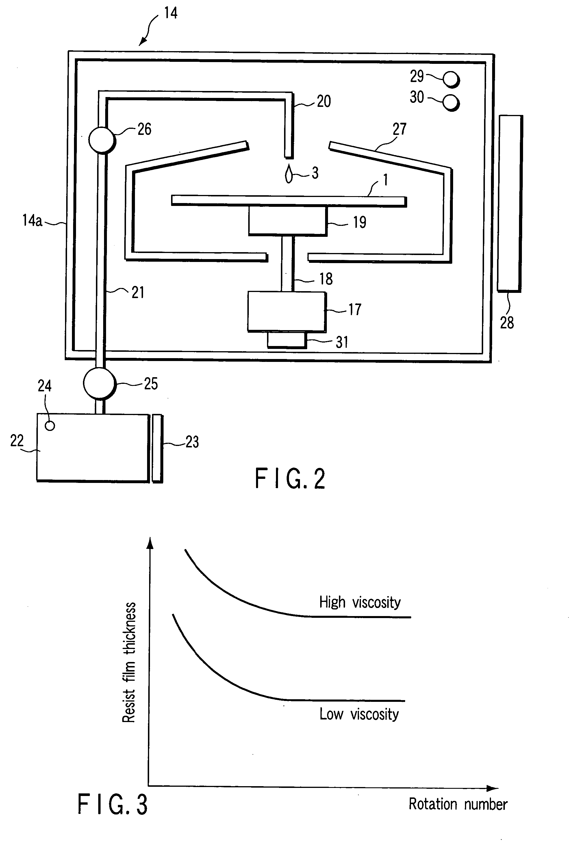
[0053] In the coater / developer 10, a coater 14, a developer 15, a reworking device 16, and first to third inspection sections 60 to 62 are disposed.

[0054] It is to be noted that as shown in FIG. 1B, a cassette C1 storing a plurality of non-defective semiconductor wafers 1, a cassette C2 storing NG semiconductor wafers 1 which cannot be re...

second embodiment

[0170] Next, the present invention will be described with reference to the drawings. It is to be noted that the same parts as those of FIG. 1 are denoted with the same reference numerals, and detailed description thereof is omitted.

[0171]FIG. 17 is a constitution diagram of a semiconductor manufacturing apparatus. A defect extraction section 100 takes in image data Im1 to Im3 acquired by the first to third inspection sections 60 to 62, respectively, and extracts defects on a semiconductor wafer 1 before the applying of a photoresist, after the applying of the photoresist, and after the exposing / developing based on the respective image data Im1 to Im3.

[0172] A defect classification section 101 obtains the following characteristic amounts of defect portions on the semiconductor wafer 1 extracted by the defect extraction section 100:

[0173] a: a characteristic amount which depends on one shot at a time when the shot of exposure light is reduced / projected onto the surface of the semico...

third embodiment

[0237]FIG. 20 is a constitution diagram showing an application example of the apparatus shown in the The respective apparatus housings 120 are arranged in such a manner that walls of a hexagonal shape are fitted into one another. The respective outlets / inlets 129 of the respective apparatus housings 120 are arranged in such a manner as to face each other, and transport paths f1, f2 of the semiconductor wafer 1 are secured.

[0238] A plurality of apparatus housings 120 are arranged in order of a film forming step of a first layer to that of an n-th layer formed on the semiconductor wafer 1. In each apparatus housing 120, a photolithography step and an etching treatment are performed to form the film of the first layer on the surface of the semiconductor wafer 1.

[0239] Moreover, the semiconductor wafer 1 is successively transported to the respective apparatus housings 120 to perform a plurality of photolithography steps and etching treatments.

[0240] To manufacture the semiconductor w...


PUM


Abstract

In a method of manufacturing a semiconductor, in which a semiconductor substrate is worked/treated in each manufacturing step of a semiconductor manufacturing line, image data is acquired before and after working/treating the semiconductor substrate transported into a manufacturing apparatus disposed in each manufacturing step, respectively, defects attributed to treatment conditions of the manufacturing apparatus are detected from the image data before the working/treating, or non-defective master image data, and the image data after the working/treating, and the treatment conditions of the manufacturing apparatus are changed/controlled based on the detection result to work/treat the semiconductor substrate.

Description

CROSS-REFERENCE TO RELATED APPLICATIONS [0001] This is a Continuation Application of PCT Application No. PCT / JP03 / 02939, filed Mar. 12, 2003, which was published under PCT Article 21(2) in Japanese. [0002] This application is based upon and claims the benefit of priority from prior Japanese Patent Application No. 2002-067374, filed Mar. 12, 2002, the entire contents of which are incorporated herein by reference.BACKGROUND OF THE INVENTION [0003] 1. Field of the Invention [0004] The present invention relates to a method and apparatus for manufacturing semiconductors for flat panel displays such as liquid crystal and plasma displays, semiconductor wafers and the like. [0005] 2. Description of the Related Art [0006]FIGS. 21A to 21G show a pre-process of manufacturing a semiconductor. An oxide film (SiO2) is formed on the surface of a semiconductor wafer 1, and a thin film 2 of silicon nitride is deposited on the oxide film. [0007] Next, the process shifts to a photolithography step, an...

Claims


Application Information

Patent Timeline
IPC IPC(8): G03F7/20H01L21/00
CPCG03F7/70991H01L21/67253H01L21/6715G03F7/7065
Inventor TANAKA, TOSHIHIKO
Owner OLYMPUS CORP
Why Eureka
Try Eureka