Plasma etching method and plasma etching unit

a plasma etching and plasma technology, applied in the direction of electrical equipment, basic electric elements, electric discharge tubes, etc., can solve the problems of poor etching geometric control performance and arisen problems, and achieve the effect of preventing charge-up damag

Inactive Publication Date: 2005-02-24
TOKYO ELECTRON LTD +1
View PDF9 Cites 44 Cited by
  • Summary
  • Abstract
  • Description
  • Claims
  • Application Information

AI Technical Summary

Benefits of technology

[0033] When the strength of the magnetic field on the focus ring is not lower than 0.001 T, drift movement of electrons may be generated on the focus ring, so that the plasma density around the focus ring is raised to make the plasma de

Problems solved by technology

However, when the etching process is conducted under the conventional relatively high pressure, although the etching selectivity of the silicon film with respect to the inorganic-material film is enhanced, an etching geometri

Method used


Image

  • Plasma etching method and plasma etching unit
  • Plasma etching method and plasma etching unit
  • Plasma etching method and plasma etching unit

Examples


Embodiment Construction

[0055] An embodiment of the invention will now be described with reference to the attached drawings.

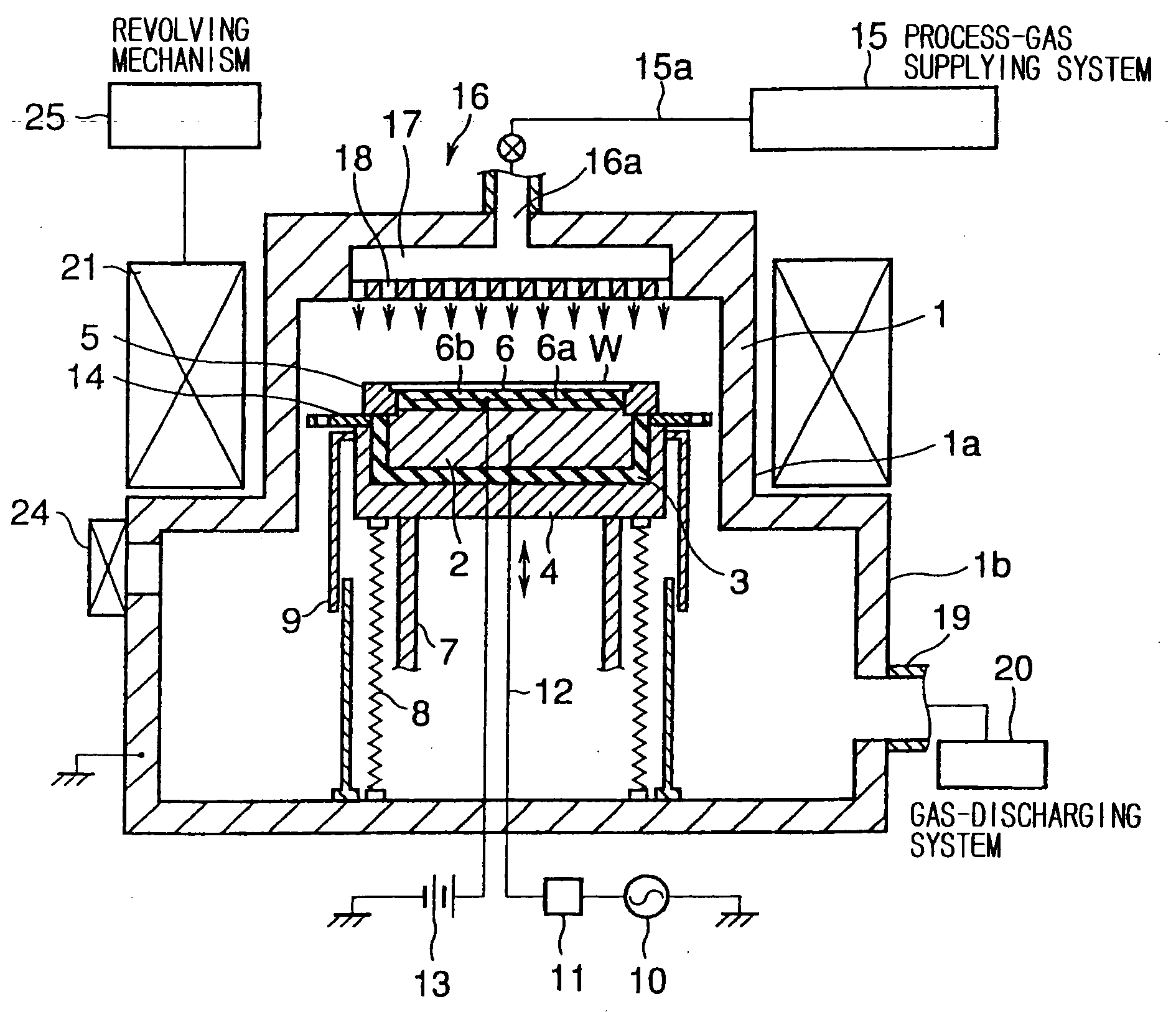
[0056]FIG. 1 is a schematic sectional view showing a plasma etching unit used for carrying out the present invention. The etching unit of the embodiment includes a two-stage cylindrical chamber vessel 1, which has an upper portion 1a having a small diameter and an lower portion 1b having a large diameter. The chamber vessel 1 may be hermetically made of any material, for example aluminum.

[0057] A supporting table 2 is arranged in the chamber vessel 1 for horizontally supporting a wafer W as a substrate to be processed. The supporting table 2 may be made of any material, for example aluminum. The supporting table 2 is placed on a conductive supporting stage 4 via an insulation plate 3. A focus ring 5 is arranged on a peripheral area of the supporting table 2. The focus ring 5 may be made of any conductive material or any insulating material. When the diameter of the wafer W is 200 mm...


PUM

PropertyMeasurementUnit
Pressureaaaaaaaaaa
Pressureaaaaaaaaaa
Pressureaaaaaaaaaa

Abstract

The present invention is a plasma etching method including: an arranging step of arranging a pair of electrodes oppositely in a chamber and making one of the electrodes support a substrate to be processed in such a manner that the substrate is arranged between the electrodes, the substrate having a silicon film and an inorganic-material film adjacent to the silicon film; and an etching step of applying a high-frequency electric power to at least one of the electrodes to form a high-frequency electric field between the pair of the electrodes, supplying a process gas into the chamber to form a plasma of the process gas by means of the electric field, and selectively plasma-etching the silicon film of the substrate by means of the plasma; wherein a frequency of the high-frequency electric power applied to the at least one of the electrodes is 50 to 150 MHz in the etching step.

Description

FIELD OF THE INVENTION [0001] The present invention relates to a plasma etching method and a plasma etching unit of plasma-etching a silicon film formed on a substrate to be processed such as a semiconductor wafer, which has the silicon film and an inorganic-material film adjacent to the silicon film. DESCRIPTION OF THE RELATED ART [0002] In a manufacturing step of a semiconductor device, a multilayer film including a silicon film, such as a poly-silicon film, and insulating films is formed on a semiconductor wafer, and then a plasma-etching process is conducted in order to form a predetermined wiring pattern. [0003] In order to conduct the plasma-etching process, various kinds of units are used. Among them, a capacitive-coupling type of parallel-plate plasma etching unit is used mainly. In the capacitive-coupling type of parallel-plate plasma etching unit, a pair of parallel-plate electrodes (upper electrode and lower electrode) are arranged in a chamber, a process gas is introduce...

Claims


Application Information

Patent Timeline
IPC IPC(8): H01L21/3065
CPCH01J37/32082H01L21/3065H01J37/3266
Inventor MATSUYAMA, SHOICHIROHONDA, MASANOBUNAGASEKI, KAZUYAHAYASHI, HISATAKA
Owner TOKYO ELECTRON LTD
Why Eureka
Try Eureka