Strained-channel fin field effect transistor (FET) with a uniform channel thickness and separate gates

a technology of fin field effect transistor and channel thickness, which is applied in the direction of transistors, semiconductor devices, electrical equipment, etc., can solve the problems of incompatibility of finfet with conventional strain silicon fabrication techniques, inability to control the thickness of the channel, and inability to use fin

Inactive Publication Date: 2005-02-24
IBM CORP
View PDF10 Cites 207 Cited by
  • Summary
  • Abstract
  • Description
  • Claims
  • Application Information

AI Technical Summary

Benefits of technology

[0009] In view of the foregoing and other exemplary problems, drawbacks, and disadvantages of the conventional methods and structures, an exemplary feature of the present invention is to provide a method (and resulting structure) for fabricating a FinFET with a strained-silicon channel.

Problems solved by technology

The fabrication of a FinFET is generally simpler than most other double-gate structures, although the channel thickness control is problematic in most known approaches (e.g., see U.S. Pat. No. 6,413,802; Yang-Kyu Choi et al., “Spacer FinFET: nanoscale double-gate CMOS technology for the terabit era”, Solid-State Electronics, 46, p.
Unfortunately, the FinFET is a non-planar device, where the plane of current conduction (i.e., the Fin) is perpendicular to the wafer surface.
This makes the FinFET non-compatible with conventional strain silicon fabrication techniques.

Method used


Image

  • Strained-channel fin field effect transistor (FET) with a uniform channel thickness and separate gates
  • Strained-channel fin field effect transistor (FET) with a uniform channel thickness and separate gates
  • Strained-channel fin field effect transistor (FET) with a uniform channel thickness and separate gates

Examples


Embodiment Construction

[0046] Referring now to the drawings, and more particularly to FIGS. 1-24, there are shown exemplary embodiments of the method and structures according to the present invention.

Exemplary Embodiments

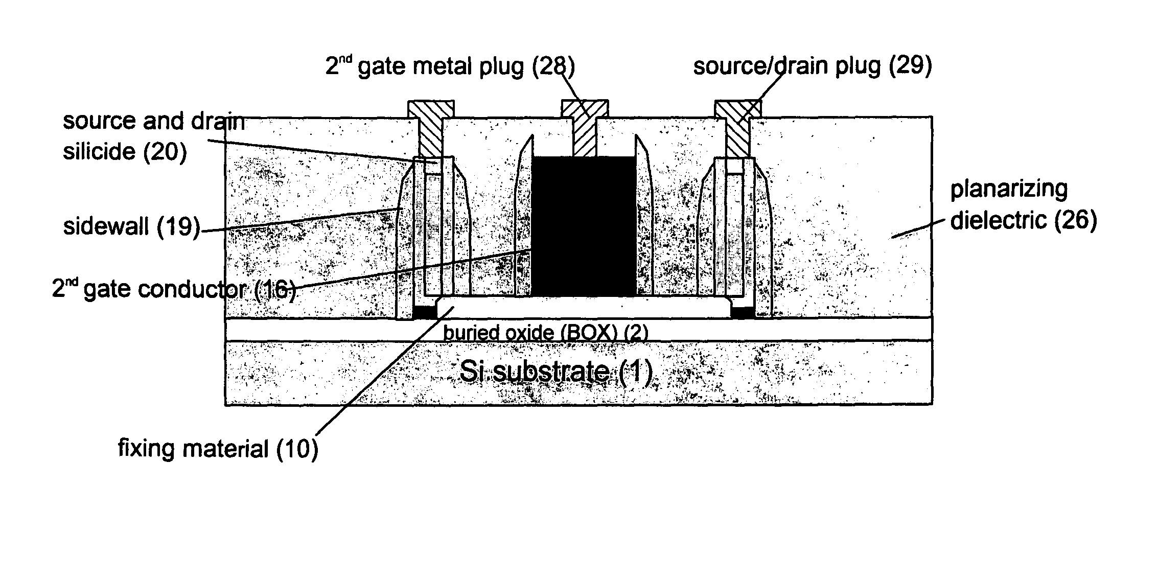
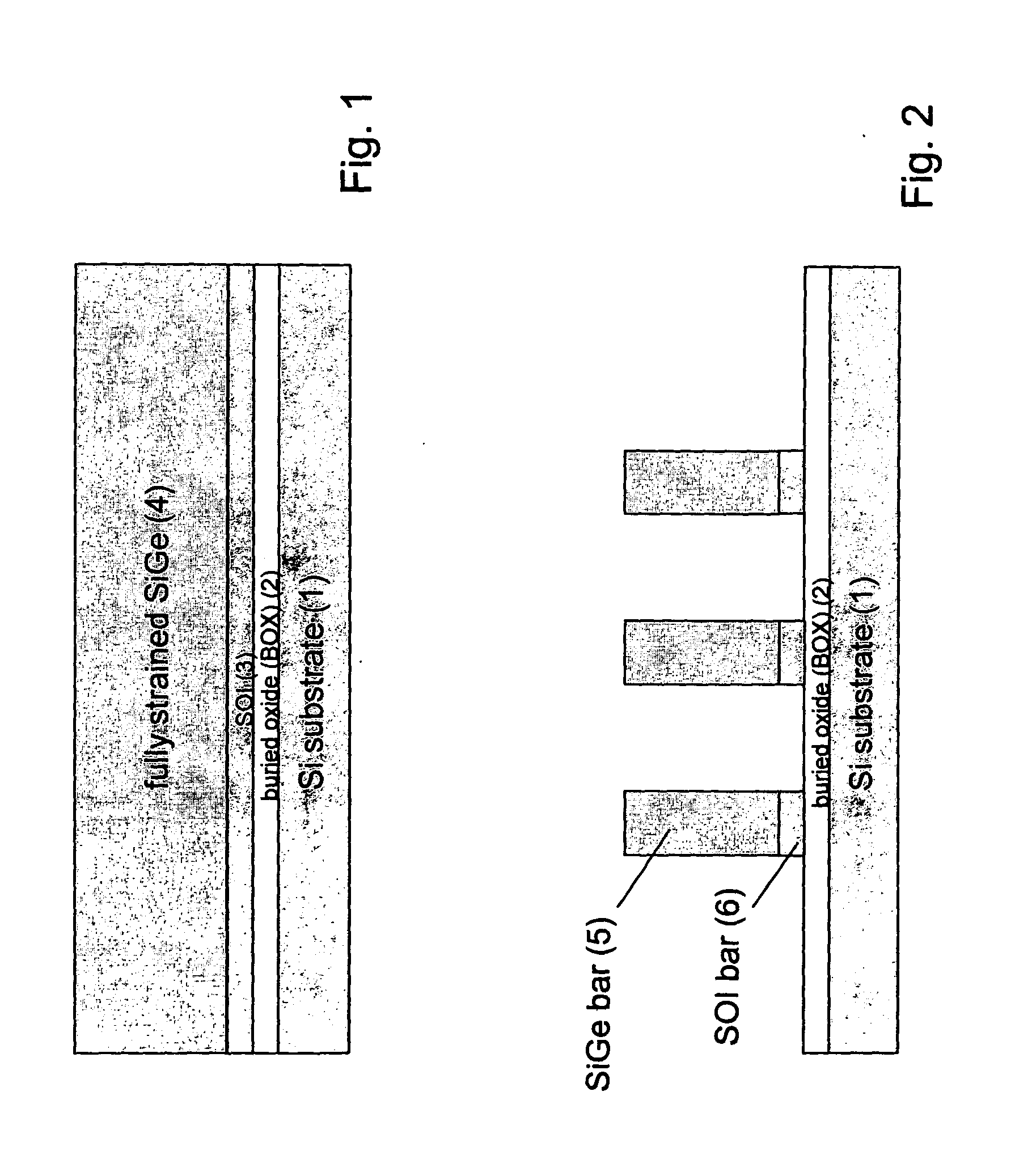
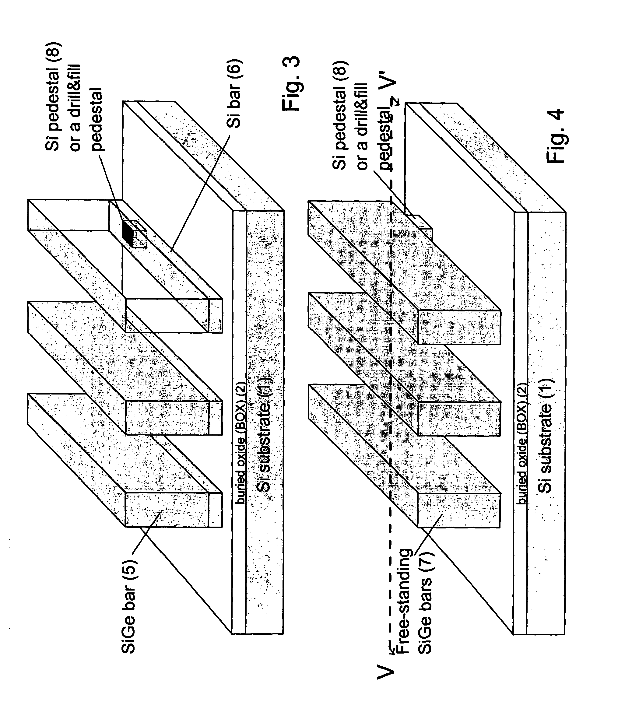
[0047] Turning to FIG. 1, FIG. 1 shows a silicon-on-insulator (SOI) substrate including a substrate 1, a buried oxide (BOX) 2 and a relatively thin SOI film 3. The buried oxide 2 may be any oxide (e.g., SiO2, etc.) material and acts as a stop etch layer, as described below. It is noted that the relatively thin SOI layer 3 is not necessarily limited to any thickness since it is a sacrificial layer, and thus can be selected based upon the designer's processing conveniences.

[0048] Then, a fully strained SiGe layer 4 is epitaxially grown on the SOI film 3. Since the SiGe layer 4 is “fully strained,” there are no defects formed therein (e.g., substantially defect-free) since the in-plane lattice constant of the SiGe 4 is matched to that of the SOI 3. Thus, the lattice mismatch between the S...


PUM


Abstract

A semiconductor device (and method for making the same) includes a strained-silicon channel formed adjacent a source and a drain, a first gate formed over a first side of the channel, a second gate formed over a second side of the channel, a first gate dielectric formed between the first gate and the strained-silicon channel, and a second gate dielectric formed between the second gate and the strained-silicon channel. The strained-silicon channel is non-planar.

Description

BACKGROUND OF THE INVENTION [0001] 1. Field of the Invention [0002] The present invention relates to a semiconductor device, and more particularly to a Fin Field Effect Transistor (FinFET) with a strained channel and electrically separate gates that are independently controllable, and to a method of forming the FinFET device. [0003] 2. Description of the Related Art [0004] FinFETs are considered promising candidates for complementary metal oxide semiconductor (CMOS) device scaling (e.g., see Hu Chenming et al., U.S. Pat. No. 6,413,802 entitled “FinFET transistor structures having a double gate channel extending vertically from a substrate and methods of manufacture”). [0005] The fabrication of a FinFET is generally simpler than most other double-gate structures, although the channel thickness control is problematic in most known approaches (e.g., see U.S. Pat. No. 6,413,802; Yang-Kyu Choi et al., “Spacer FinFET: nanoscale double-gate CMOS technology for the terabit era”, Solid-State...

Claims


Application Information

Patent Timeline
Patent Type & Authority Applications(United States)
IPC IPC(8): H01L27/08H01L21/336H01L21/8234H01L21/84H01L27/088H01L27/092H01L27/12H01L29/10H01L29/786
CPCH01L21/823412H01L21/823487H01L21/84H01L27/1203H01L29/1054H01L29/66795H01L2924/0002H01L29/7842H01L29/785H01L29/78687H01L2924/00H01L27/092
Inventor COHEN, GUY MOSHE
Owner IBM CORP
Why Eureka
Try Eureka