Electro-optical device and electronic apparatus device

a technology of optical devices and electronic apparatus, applied in the direction of static indicating devices, discharge tubes luminescnet screens, instruments, etc., can solve the problems of easy rubbing, light leakage, display defects, etc., and achieve the effect of preventing contrast reduction

Active Publication Date: 2005-02-24
BOE TECH GRP CO LTD
View PDF2 Cites 62 Cited by
  • Summary
  • Abstract
  • Description
  • Claims
  • Application Information

AI Technical Summary

Benefits of technology

[0046] In such a method of manufacturing an electro-optical device, when the alignment marks are previously formed at appropriate positions on one substrate and the R, G, and B colored layers are formed at the desired positions, the positions of the spacers are determined based on the alignment marks. In addition, when the spacers are formed by a photolithography process after the colored layers are formed, the positions of the spacers are determined by the same alignment

Problems solved by technology

When the spacers are formed by a photolithography process in this way, the alignment of liquid crystal molecules is disturbed around the spacers, and thus a display defect, such as light leakage, may easily occur.
When rubbing is performe

Method used


Image

  • Electro-optical device and electronic apparatus device
  • Electro-optical device and electronic apparatus device
  • Electro-optical device and electronic apparatus device

Examples


first embodiment

[0067] First Embodiment of Electro-Optical Device

[0068] As an example of an electro-optical device according to the present invention, a transflective liquid crystal device in which a thin film diode (TFD) element is used as an active element will now be described. Herein, the transflective method is a display method which performs both reflective display and transmissive display, wherein reflective display is performed by reflecting external light, such as sunlight or indoor light, from a reflective layer, and transmissive display is performed using light emitted from a backlight towards a substrate. In addition, it is obvious that the electro-optical device to which the present invention is applicable is not limited to the present embodiment.

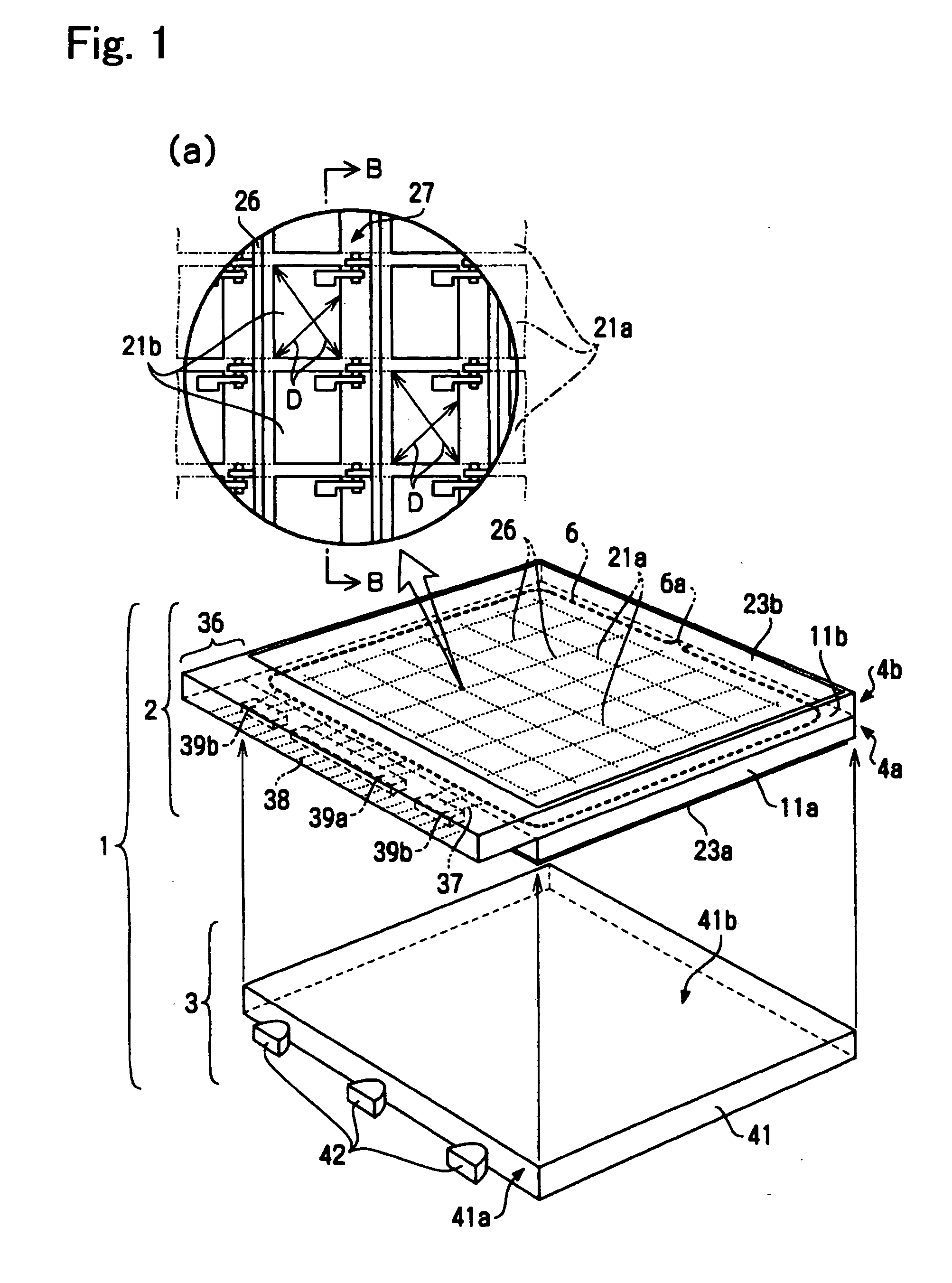
[0069] In FIG. 1, a liquid crystal device 1 includes a liquid crystal display panel 2 and an illuminating device 3 mounted on the liquid crystal display panel 2. The liquid crystal display panel 2 is formed by attaching a first substrate 4a t...

second embodiment

[0098] Second Embodiment of Electro-Optical Device

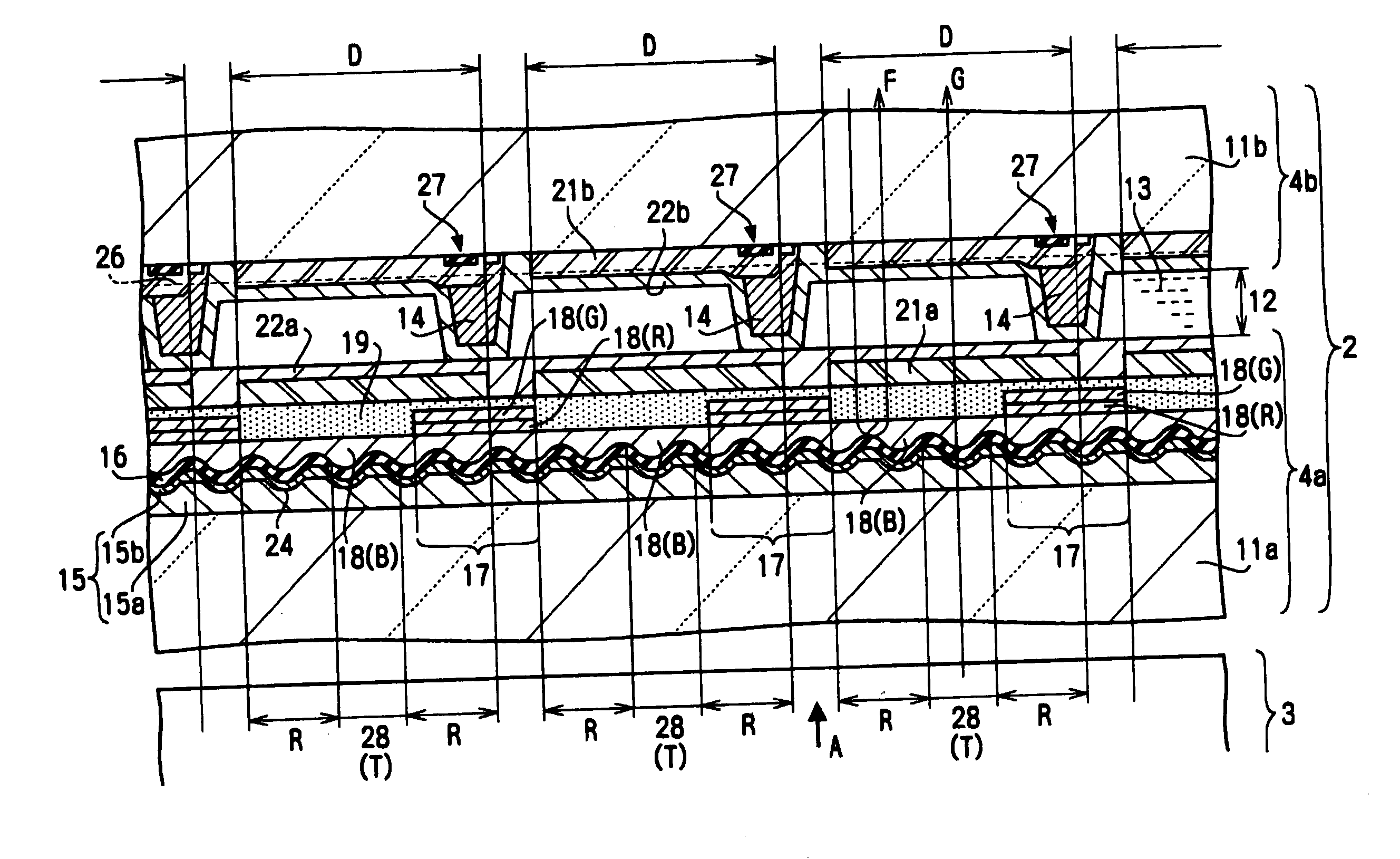
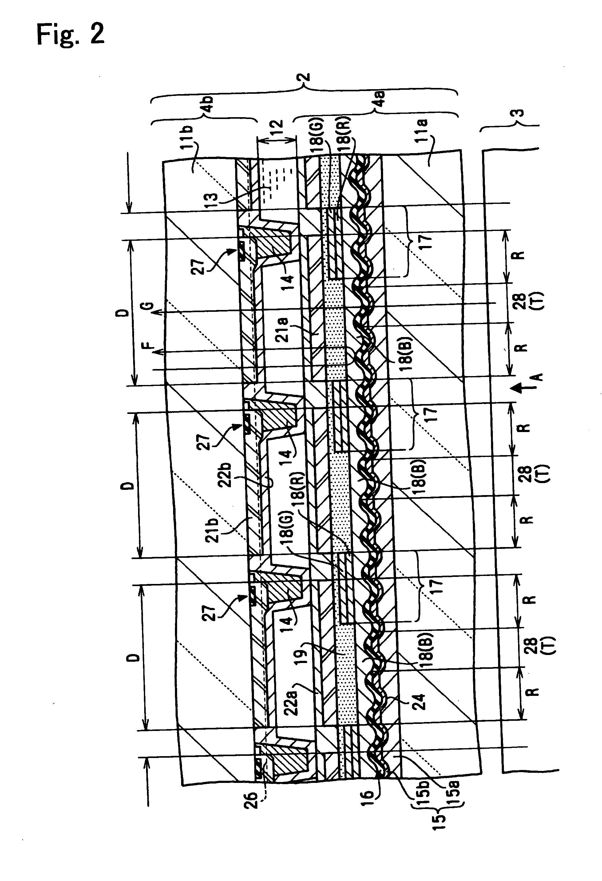
[0099] In the aforementioned embodiment, as shown in FIG. 4, the spacers 14 are formed in the cut-out regions of the B colored layers 18(B), that is, in regions corresponding to active element-forming regions. Alternatively, the spacers 14 may be formed in the cut-out regions of the R colored layers 18(R). Since the brightness of display is such that G>R>B as described above, a reduction in contrast can be prevented even if a positional deviation occurs between the substrates, compared to a case where the spacers 14 get into the G colored regions.

[0100] In addition, as can easily be seen from FIG. 4, in a stripe arrangement of R, G, and B colors used in the present embodiment, the B colored regions are situated in the vicinity of the cut-out regions of the R colored layers 18(R), but the G colored regions are not situated therein. Thus, according to the present embodiment in which the spacers 14 are formed in the cut-out regions of ...

third embodiment

[0101] Third Embodiment of Electro-Optical Device

[0102]FIG. 6 shows an electro-optical device according to still another embodiment of the present invention. In particular, FIG. 6 shows the positional relationship between the spacers 14 and the colored layers 18. The liquid crystal device of FIG. 6 includes the colored layers 18 of R, G, and B colors aligned in a stripe arrangement. In the present embodiment, the spacers 14 are formed at positions corresponding to a light-shielding layer 17 around the B colored layers 18(B), but are not formed at positions corresponding to the light-shielding layer 17 around the G colored layers 18(G).

[0103] In addition, in the present embodiment, the spacers 14 are formed in the light-shielding layer 17 between a plurality of adjacent B colored layers 18(B) arranged in a line in the lengthwise direction, but are not formed in the light-shielding layer 17 around the G colored layers 18(G).

[0104] According to this arrangement for the spacers 14, ev...


PUM


Abstract

A liquid crystal device is provided that comprises a plurality of R colored layers, a plurality of G colored layers, and a plurality of B colored layers that are formed on either one of a pair of substrates and are aligned in a predetermined arrangement in plan view, a light-shielding layer formed between the colored layers, and a plurality of spacers formed on either one of the pair of substrates and protruding toward the other substrate. The plurality of spacers is formed around the B colored layers and/or the R colored layers, but is not formed around the G colored layers. Thus, even if a positional deviation occurs between the substrates, the spacers do not get into the G colored layers.

Description

RELATED APPLICATIONS [0001] This application claims priority to Japanese Patent Application No. 2003-137529 filed May 15, 2003 which is hereby expressly incorporated by reference herein in its entirety. BACKGROUND OF THE INVENTION [0002] 1. Technical Field of the Invention [0003] The present invention relates to an electro-optical device comprising color filters composed of R (red), G (green), and B (blue) colored layers and a plurality of spacers formed by a pattern-forming method such as a photolithography process, and to an electronic apparatus. [0004] 2. Description of the Related Art [0005] In general, in a liquid crystal device, a liquid crystal layer is interposed between a pair of substrates, the alignment of liquid crystal molecules in the liquid crystal layer is controlled in each display dot, which is a minimum unit of display, and light passing through the liquid crystal layer is modulated in each display dot by the liquid crystal molecules, thereby displaying an image, ...

Claims


Application Information

Patent Timeline
IPC IPC(8): G02B5/23G02F1/133G02F1/1339G02F1/1335G09G3/36H01J1/62H01J63/04
CPCG02F1/133512G02F1/13394G02F1/133514H04M1/0214H04M1/0225
Inventor TAGUCHI, SATOSHIASADA, KOJIKAMIJIMA, MOTOHIRO
Owner BOE TECH GRP CO LTD
Why Eureka
Try Eureka