Device package with hermetically sealed cap and device encapsulation method
- Summary
- Abstract
- Description
- Claims
- Application Information
AI Technical Summary
Benefits of technology
Problems solved by technology
Method used
Image

Examples
first embodiment
[0016] [First Embodiment]
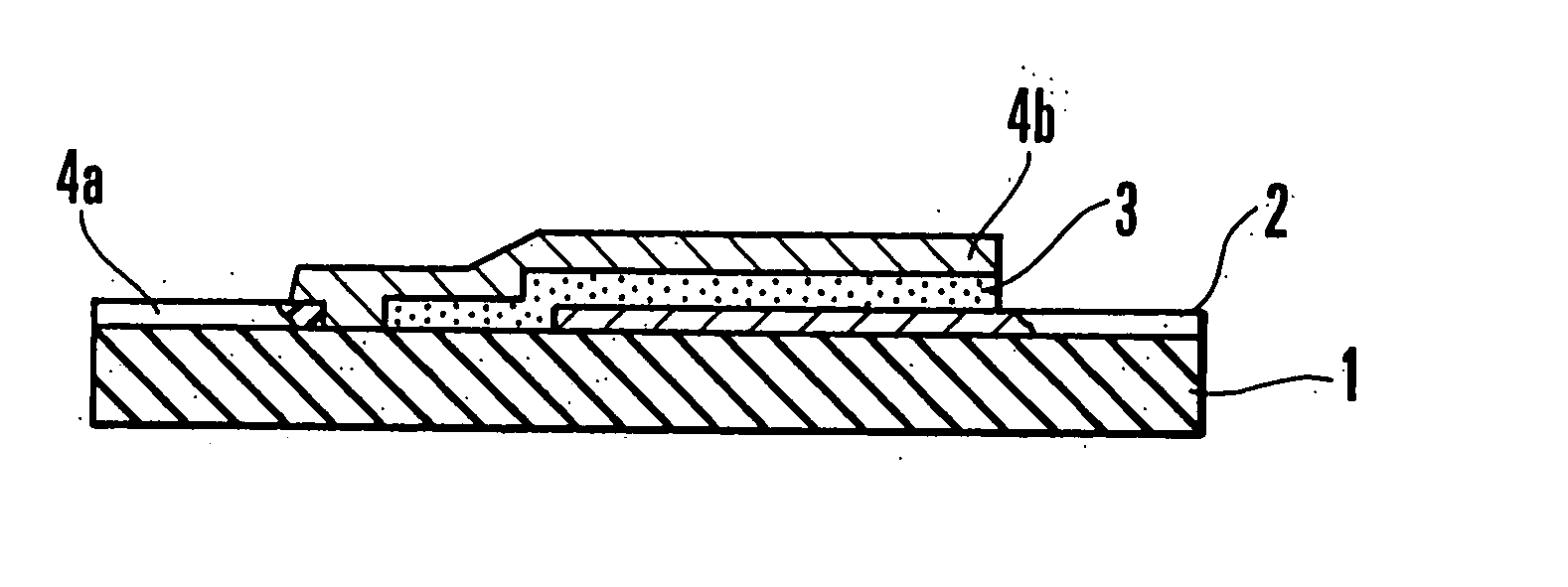
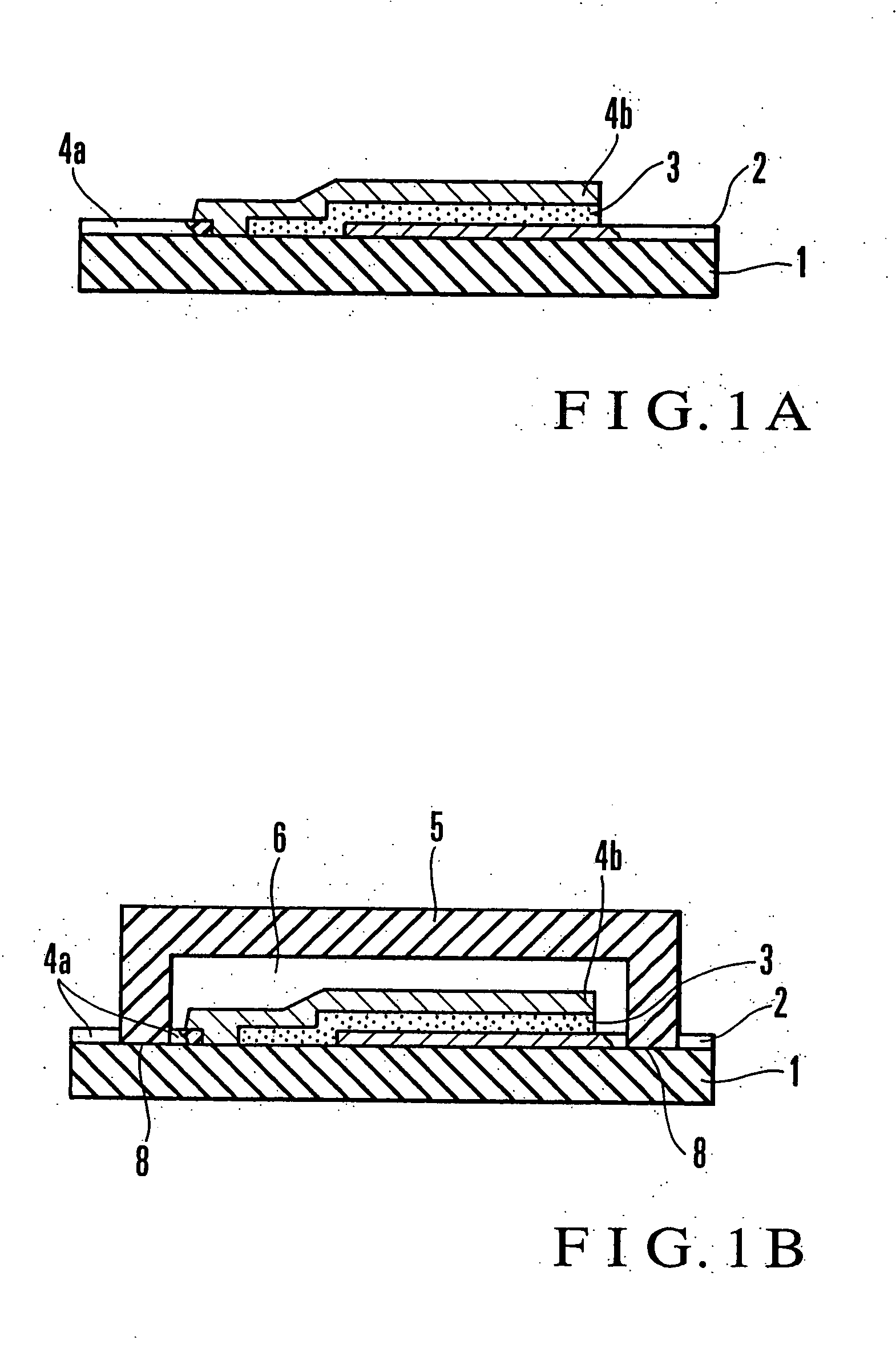
[0017]FIGS. 1A and 1B show the steps in manufacturing an organic EL device according to the first embodiment of the present invention. In FIGS. 1A and 1B, the respective portions are illustrated with easily recognizable sizes for the sake of illustrative convenience and accordingly have a film ratio different from the actual one.
[0018] As shown in FIG. 1A, an anode 2 and a cathode 4a each formed of an ITO film, an organic EL device 3, and a metal cathode 4b are sequentially formed on a substrate 1. As shown in FIG. 1B, a box- or dome-shaped encapsulation cap 5 made of the same material as that of the substrate 1 and having one open surface is placed on the substrate 1, and its end face and the substrate 1 are welded by using ultrasonic welding. The encapsulation cap 5 has such a shape that it can maintain a hollow portion 6, so that it will not come into direct contact with the cathode 4b. The hollow portion 6 is filled with a gas containing neither oxygen ...
second embodiment
[0034] [Second Embodiment]
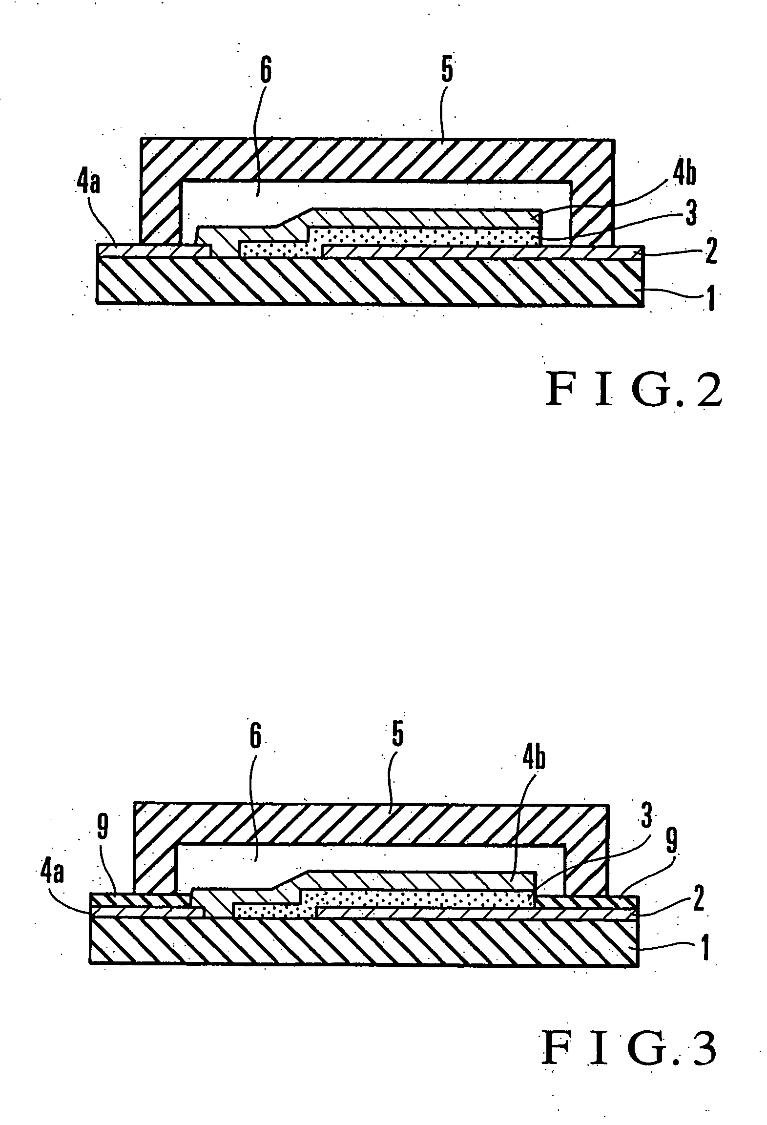
[0035] As the second embodiment, in FIG. 3, in order to improve the adhesion properties of welding of a substrate 1 and an encapsulation cap 5, a resin layer 9 made of the same material as that of the substrate 1 is formed by coating in advance on an anode 2 and a cathode 4a that are present between the substrate 1 and encapsulation cap 5. The substrate 1 and encapsulation cap 5 are then welded to each other. At this time, the encapsulation cap 5 is welded to the resin layer 9 at regions on the anode 2 and cathode 4a.
[0036] A result obtained by evaluating the organic EL device of this embodiment in accordance with the same method as in the first embodiment is as follows. In contrast to an initial non-emission area ratio of 0.5%, the non-emission area ratio obtained after the organic EL device was left to stand for 500 hours at 50° C. in the 90% RH atmosphere without being driven was 0.7%. Regarding the dark spot diameter, in contrast to an initial value of...
third embodiment
[0038] [Third Embodiment]
[0039]FIG. 4 shows an organic EL device according to the third embodiment of the present invention. In FIG. 4, portions having the same arrangement as those of FIG. 1B are denoted by the same reference numerals as in FIG. 1B. In the third embodiment, an active carbon layer 7 is formed on the inner wall of an encapsulation cap 5, and thereafter a substrate 1 and the encapsulation cap 5 are welded to each other. This can improve the contrast of organic EL emission, in the same manner as in the above modification. Since a fusion gas generated during ultrasonic welding of the substrate 1 and encapsulation cap 5 is adsorbed by the active carbon layer 7, the service life of the organic EL device can be further prolonged.
[0040] A result obtained by evaluating the organic EL device of this embodiment in accordance with the same method as in the first embodiment is as follows. In contrast to an initial non-emission area ratio of 0.4%, the non-emission area ratio obt...
PUM
 Abstract
Description
Claims
Application Information
 - R&D
- Intellectual Property
- Life Sciences
- Materials
- Tech Scout
- Unparalleled Data Quality
- Higher Quality Content
- 60% Fewer Hallucinations
Browse by: Latest US Patents, China's latest patents, Technical Efficacy Thesaurus, Application Domain, Technology Topic, Popular Technical Reports.
© 2025 PatSnap. All rights reserved.Legal|Privacy policy|Modern Slavery Act Transparency Statement|Sitemap|About US| Contact US: help@patsnap.com