Nram bit selectable two-device nanotube array

a nanotube array and nanotube technology, applied in the field of nonvolatile ram structures, can solve the problems of slow speed relative to dram or sram, long write cycles (ms), and low cost of rom,

Inactive Publication Date: 2005-02-24
NANTERO
View PDF42 Cites 100 Cited by
  • Summary
  • Abstract
  • Description
  • Claims
  • Application Information

AI Technical Summary

Problems solved by technology

ROM is relatively low cost but cannot be rewritten.
However, EPROM exhibits a reliability limited to a few iterative read / write cycles and long erase times. EEPROM has low power consumption and is inexpensive, but has long write cycles (ms) and slow speed relative to DRAM or SRAM.
Flash memory is faster than EEPROM but still incurs the same detriments as EEPROM.
Flash memory also has a finite number of read / write cycles giving rise to low long-term reliability.
Yet, SRAM has lower density and higher cost than DRAM.
Volatile memory loses information stored in the memory cells, if an interruption in power occurs.
Non-volatile memories are not randomly accessible and do not support multiple writes with any high degree of reliability.
In addition, non-volatile memories have low density and high cost.
Volatile memories have either complicated system design or have low density.
A different memory cell based upon magnetic tunnel junctions has also been examined but has not led to large-scale commercialized MRAM devices.
FRAM suffers from a large memory cell size, and it is difficult to manufacture as a large-scale integrated component.
Unfortunately, phase change memory suffers from slow operations and questionable reliability.
Phase change memory is also difficult to manufacture and, consequently, has not been commercialized.
Inherent within redox processes, this form of memory can be unstable (volatile) and requires highly specialized wire junctions.
These techniques are now believed to be difficult to employ at commercial scales using modern technology.
Moreover, they may contain inherent limitations such as the length of the nanotubes that may be grown reliably using these techniques, and it may difficult to control the statistical variance of geometries of nanotube wires so grown.

Method used


Image

  • Nram bit selectable two-device nanotube array
  • Nram bit selectable two-device nanotube array
  • Nram bit selectable two-device nanotube array

Examples


Embodiment Construction

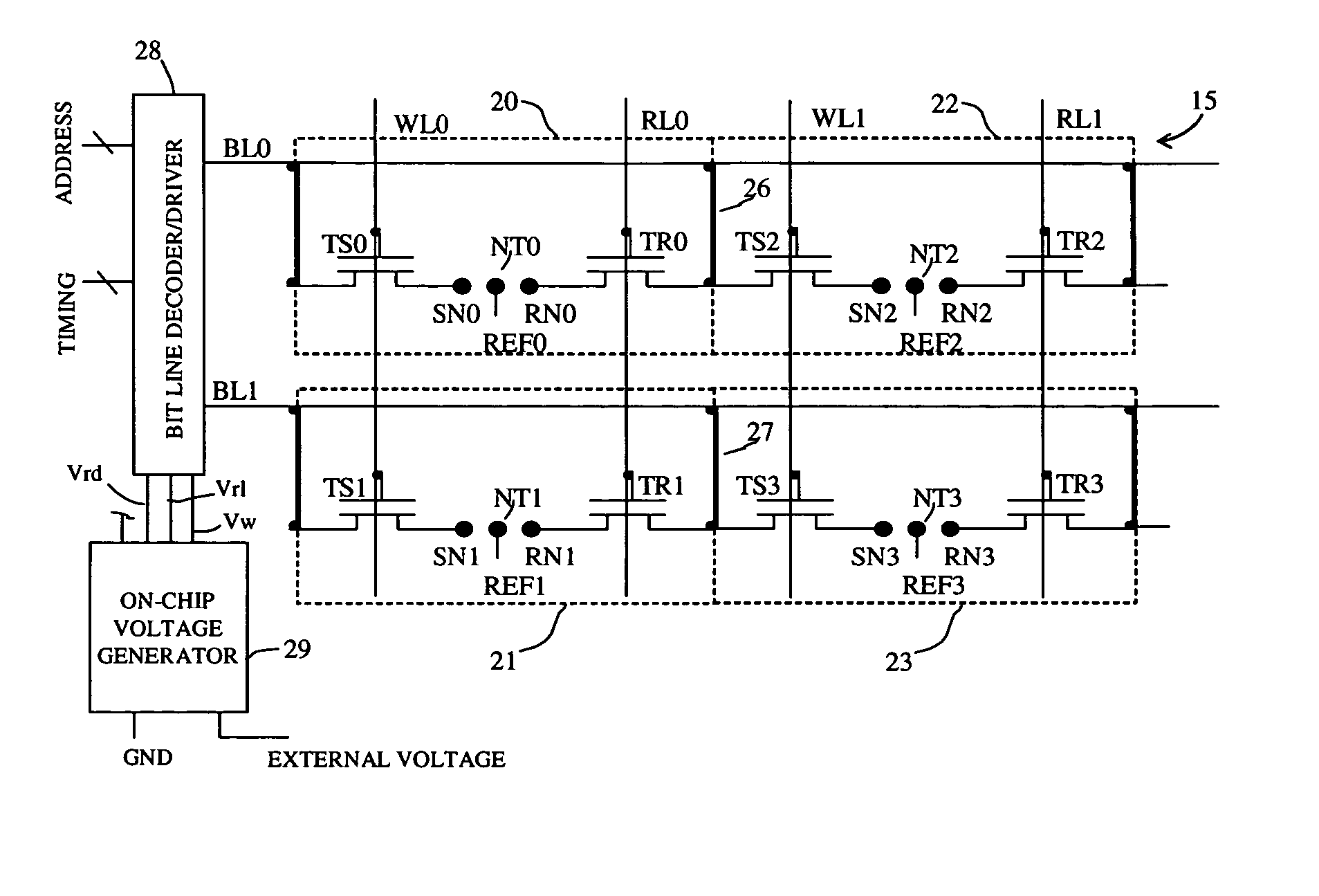
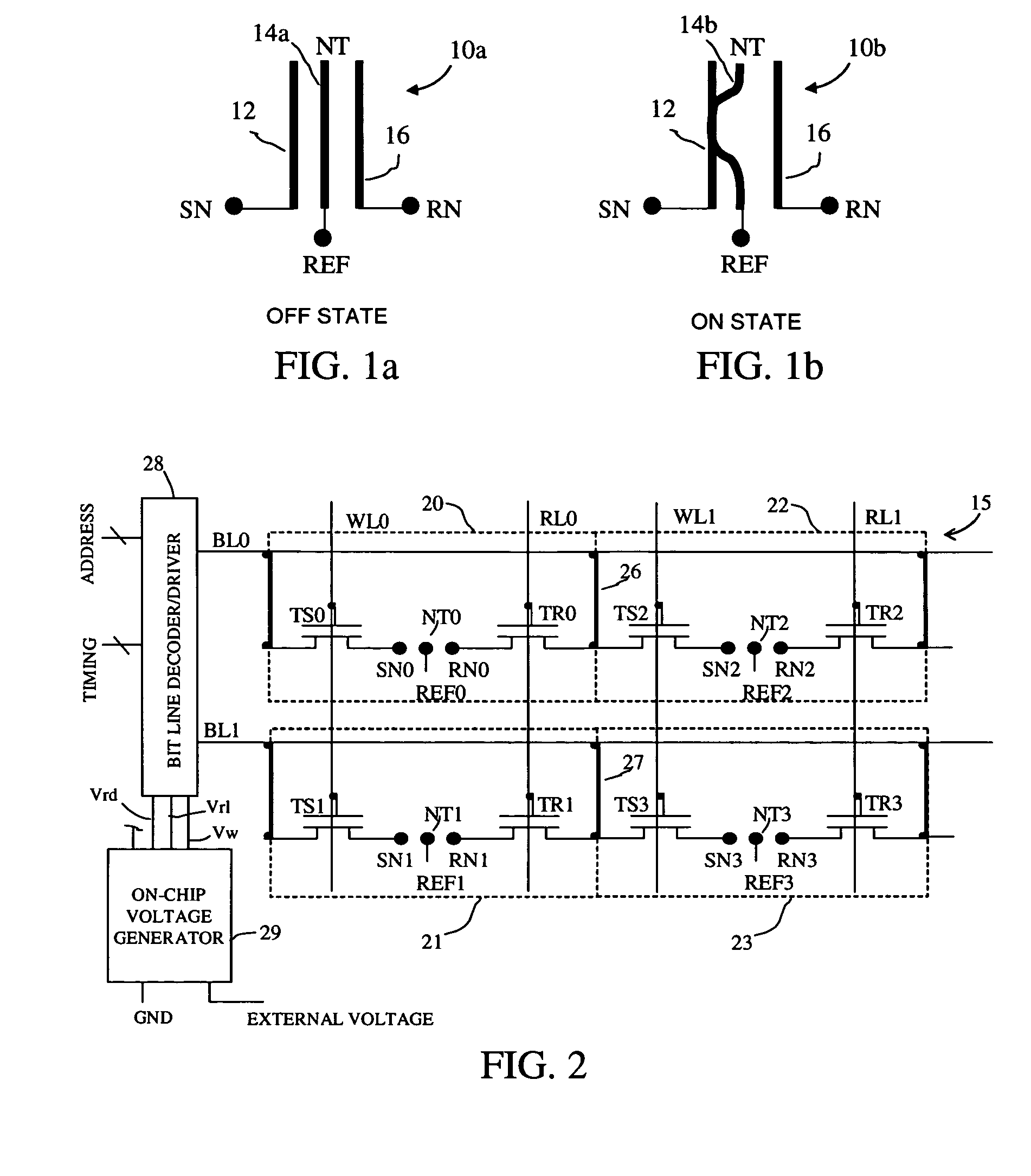
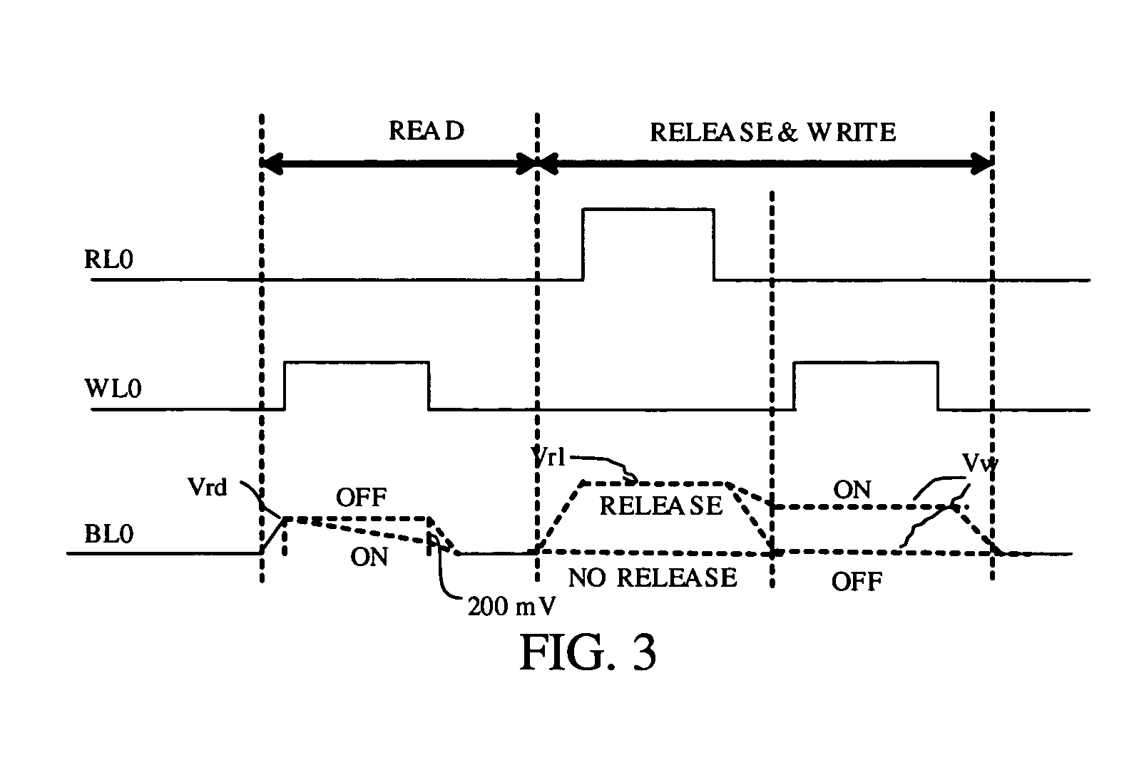
[0041] Preferred embodiments of the invention provide a non-volatile ram cell and array structure in which information state is manifested by the physically deflected position of a nanotube (NT) switching element. The non-volatile ram cells are bit selectable for read and write operations. The NT switching component has two states: an On state and an Off state. The NT element may be caused to deflect to one state or the other through transistor interface circuitry; that is, the surrounding circuit does not access the NT element directly but instead accesses transistor devices to set or release the NT element from one state or the other.

[0042]FIGS. 1A and B depict an NT switching element. The devices include a set node 12 a release node 16 and a nanotube element positioned in between. The NT element generally extends perpendicularly to the nodes 12 and 16. In preferred embodiments the NT element is formed from a fabric of nanotubes, as is described further below. The NT element in t...


PUM


Abstract

A non-volatile memory array includes a plurality of memory cells, each cell receiving a bit line, word line, and release line. Each memory cell includes a cell selection transistor and a restore transistor with first, second and third nodes. Each cell further includes an electromechanically deflectable switch, the position of which manifests the logical state of the cell. Each cell is bit selectable for read and write operations.

Description

CROSS-REFERENCE TO RELATED APPLICATIONS [0001] This application claims priority under 35 U.S.C. § 119(e) to U.S. Provisional Apl. Ser. No. 60 / 459,223, filed on Mar. 28, 2003, entitled NRAM BIT SELECTABLE TWO-DEVICE NANOTUBE ARRAY, which is expressly incorporated herein by reference in its entirety. [0002] This application is related to the following U.S. applications, the contents of which are incorporated herein in their entirety by reference: [0003] U.S. Provisional Apl. Ser. No. 60 / 459,222 filed on Mar. 28, 2003, entitled NRAM Bit Selectable One-Device Nanotube Array; and U.S. patent application Ser. No. (inserted upon USPTO designation), filed on the same day as the present application, entitled Non-Volatile Ram Cell And Array Using Nanotube Switch Position For Information State. [0004] U.S. Provisional Patent Application No. 60 / 459,253, filed on Mar. 28, 2003, entitled Single Transistor with Integrated Nanotube (NT-FET); and U.S. patent application Ser. No. (inserted upon USPTO...

Claims


Application Information

Patent Timeline
Patent Type & Authority Applications(United States)
IPC IPC(8): G11C13/02G11C23/00
CPCB82Y10/00Y10S977/943G11C23/00G11C13/025
Inventor RUECKES, THOMASSEGAL, BRENT M.VOGELI, BERNHARDBROCK, DARREN K.JAIPRAKASH, VENKATACHALAM C.BERTIN, CLAUDE L.
Owner NANTERO
Why Eureka
Try Eureka