Ferroelectric memory and method for manufacturing the same
a technology of ferroelectric memory and manufacturing method, which is applied in the direction of digital storage, capacitors, instruments, etc., can solve the problems of reduction of polarizability or voltage endurance, and deterioration of the characteristics of the ferroelectric film, so as to improve the reduction resistance of the capacitive element
- Summary
- Abstract
- Description
- Claims
- Application Information
AI Technical Summary
Benefits of technology
Problems solved by technology
Method used
Image

Examples
first embodiment
[0121] (First Embodiment)
[0122] A ferroelectric memory according to a first embodiment of the present invention, and a method for manufacturing the same, will now be described with reference to the drawings.
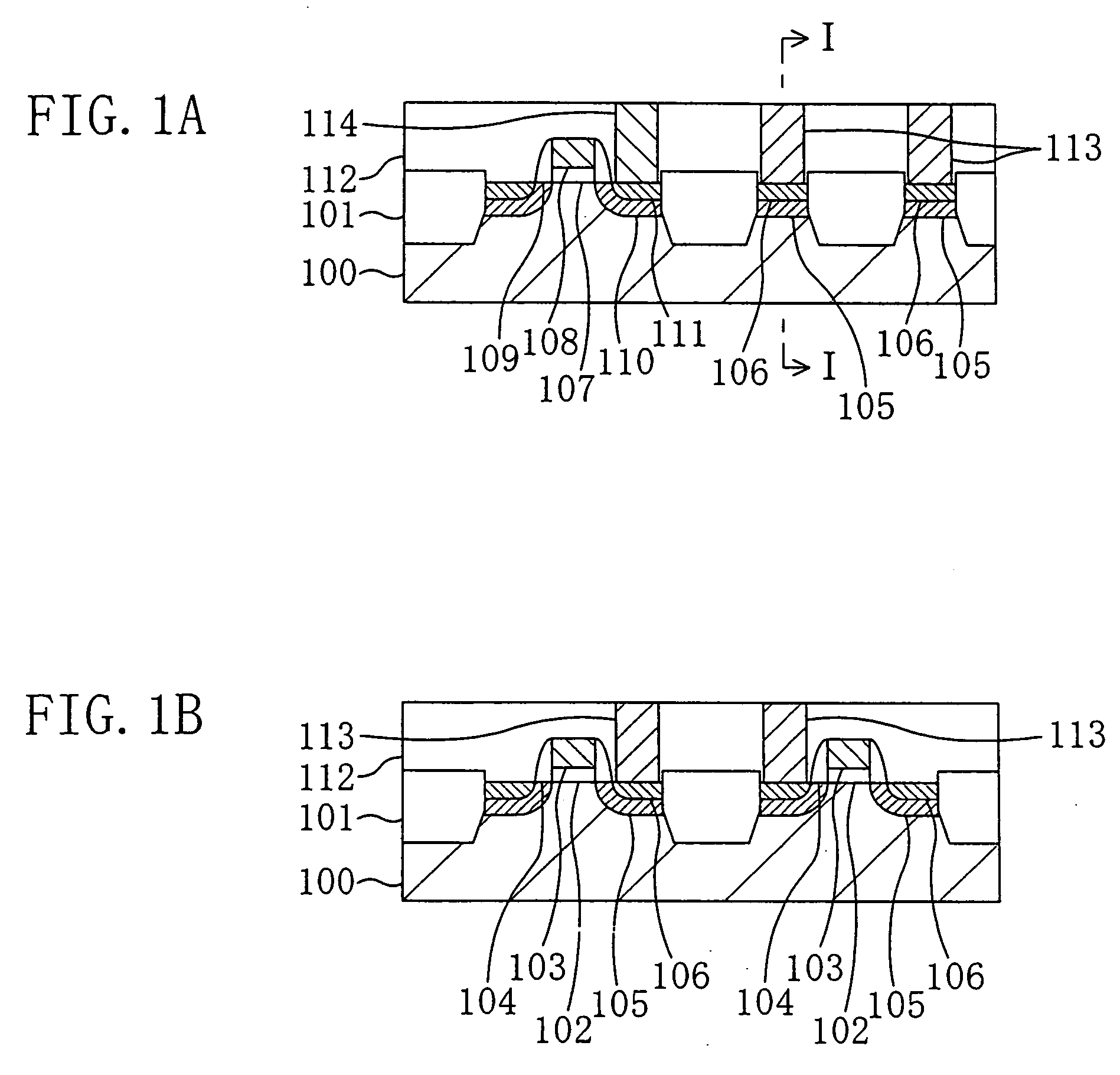
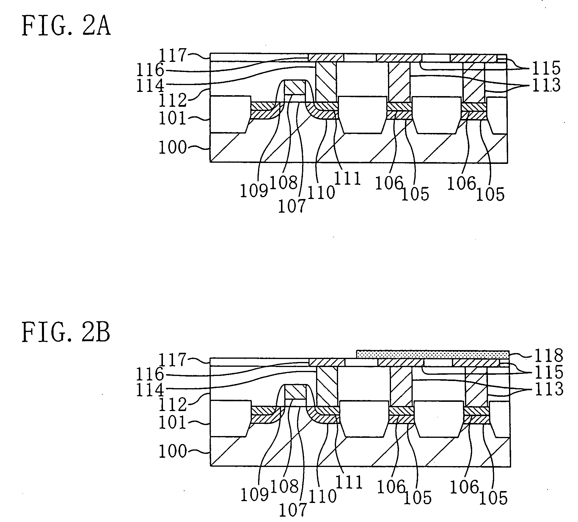
[0123]FIG. 1A, FIG. 1B, FIG. 2A, FIG. 2B, FIG. 3A to FIG. 3C, FIG. 4A and FIG. 4B are cross-sectional views each illustrating a step in a method for manufacturing a ferroelectric memory according to the first embodiment. Note that FIG. 1B is a cross-sectional view taken along line I-I in FIG. 1A, and FIG. 4B is a cross-sectional view taken along line IV-IV in FIG. 4A.
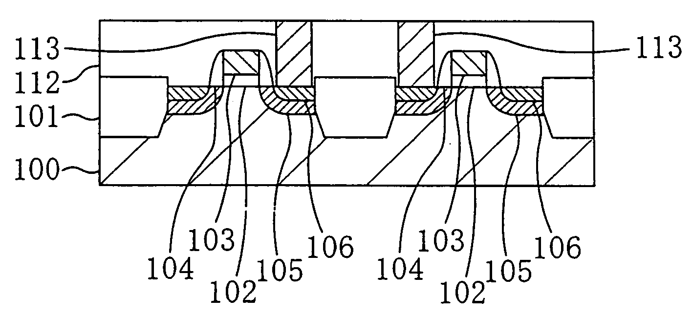
[0124] First, as illustrated in FIG. 1A and FIG. 1B, a device isolation region 101 having an STI structure is formed on the surface of a semiconductor substrate 100. Then, in a region where a memory cell is to be formed (hereafter referred to as a “memory cell region”) within each region of the semiconductor substrate 100 surrounded by the device isolation region 101, a first gate electrode 103 forming a part of a ...
second embodiment
[0204] (Second Embodiment)
[0205] A ferroelectric memory according to a second embodiment of the present invention, and a method for manufacturing the same, will now be described with reference to the drawings.
[0206]FIG. 13A, FIG. 13B, FIG. 14A, FIG. 14B, FIG. 15A to FIG. 15C, FIG. 16A and FIG. 16B are cross-sectional views each illustrating a step in a method for manufacturing a ferroelectric memory according to the second embodiment. Note that FIG. 13B is a cross-sectional view taken along line XIII-XIII in FIG. 13A, and FIG. 16B is a cross-sectional view taken along line XVI-XVI in FIG. 16A.
[0207] First, as illustrated in FIG. 13A and FIG. 13B, a device isolation region 201 having an STI structure is formed on the surface of a semiconductor substrate 200. Then, on a memory cell region within each region of the semiconductor substrate 200 surrounded by the device isolation region 201, a first gate electrode 203 forming a part of a memory cell transistor is formed via a first gate...
third embodiment
[0238] (Third Embodiment)
[0239] A ferroelectric memory according to a third embodiment of the present invention, and a method for manufacturing the same, will now be described with reference to the drawings.
[0240]FIG. 21A, FIG. 21B, FIG. 22A, FIG. 22B, FIG. 23A to FIG. 23C, FIG. 24A and FIG. 24B are cross-sectional views each illustrating a step in a method for manufacturing a ferroelectric memory according to the third embodiment. Note that FIG. 21B is a cross-sectional view taken along line XXI-XXI in FIG. 21A, and FIG. 24B is a cross-sectional view taken along line XXIV-XXIV in FIG. 24A.
[0241] First, as illustrated in FIG. 21A and FIG. 21B, a device isolation region 301 having an STI structure is formed on the surface of a semiconductor substrate 300. Then, a gate electrode 303 forming a part of a memory cell transistor is formed via a gate insulating film 302 on a memory cell region within each region of the semiconductor substrate 300 surrounded by the device isolation region...
PUM
 Abstract
Description
Claims
Application Information
 - R&D
- Intellectual Property
- Life Sciences
- Materials
- Tech Scout
- Unparalleled Data Quality
- Higher Quality Content
- 60% Fewer Hallucinations
Browse by: Latest US Patents, China's latest patents, Technical Efficacy Thesaurus, Application Domain, Technology Topic, Popular Technical Reports.
© 2025 PatSnap. All rights reserved.Legal|Privacy policy|Modern Slavery Act Transparency Statement|Sitemap|About US| Contact US: help@patsnap.com