Image sensor with improved uniformity of effective incident light

a technology of effective incident light and image sensor, which is applied in the field of image sensors, can solve the problems of limited fill factor increase and especially problematic phenomenon, and achieve the effect of improving the issue of non-uniform incident ligh

Active Publication Date: 2005-03-03
TAIWAN SEMICON MFG CO LTD
View PDF4 Cites 8 Cited by
  • Summary
  • Abstract
  • Description
  • Claims
  • Application Information

AI Technical Summary

Benefits of technology

[0010] Accordingly, it is the object of this invention to provide an image sensor that obtains more uniform photoenergy in different regions of the chip, especially the center region and the edge region.
[0011] It is another object of this invention to provide an image sensor that avoids the cross-talk problem.
[0013] In another embodiment of the present invention, an image sensor is designed following the condition that the distance between a center of the microlens and a center of a corresponding sensing area is a function of the distance between the corresponding sensing area, such as a photodiode, to a chip center, and each microlens is disposed overlying a corresponding color filter unit without overlying adjacent color filters. Therefore, the issue of non-uniform incident light is improved.

Problems solved by technology

Although efforts have been made to increase the fill factor of the image sensor and thereby increase the sensor sensitivity, further increases in the fill factor are limited because the associated logic circuitry cannot be completely removed.
The phenomenon is especially problematic for microlenses 21 disposed near the edge region of the sensor chip 10.

Method used


Image

  • Image sensor with improved uniformity of effective incident light
  • Image sensor with improved uniformity of effective incident light
  • Image sensor with improved uniformity of effective incident light

Examples


first embodiment

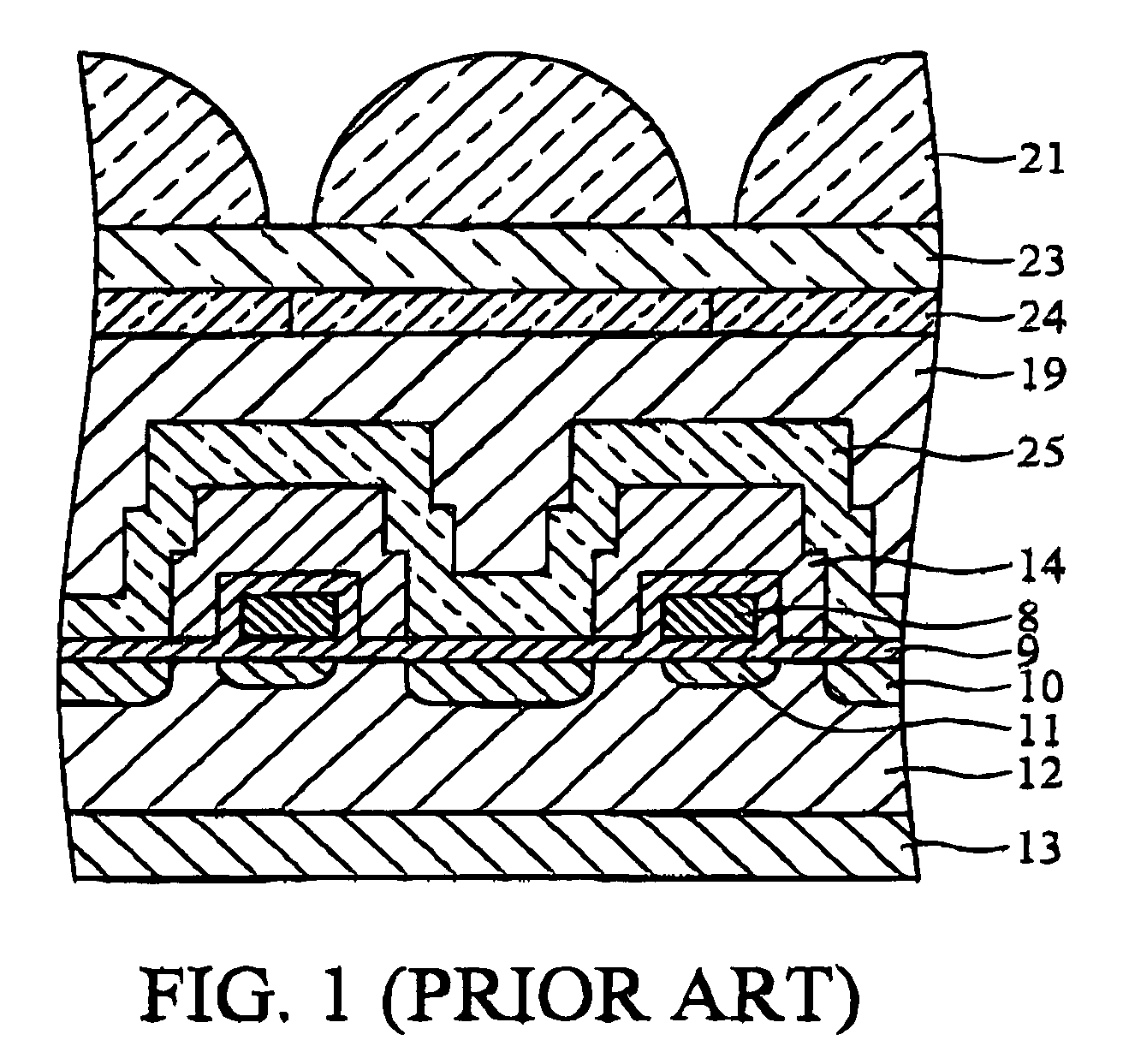
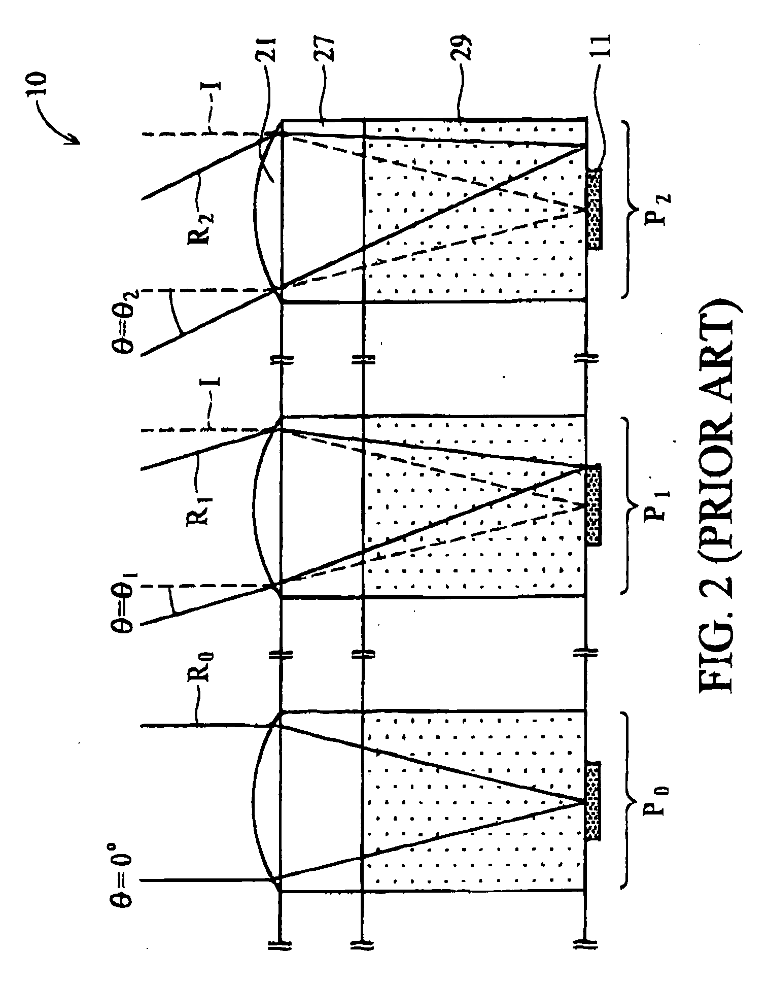
[0019] The incident light transmitted into the microlenses and ranching the sensing areas of an image sensor may not uniformly collimated light, especially for the regions away from the chip center. Therefore the image displayed on the edge region is darker than the center region.

[0020] The present invention provides a method improving the uniformity of effective incident light and avoiding cross-talk between adjacent pixels in a chip equipped with an image sensor so as to balance the brightness in different regions. The microlens layer consists of a plurality of microlenses corresponding to a plurality of sensing areas, respectively. The size of microlens is a function of the distance between microlens to the chip center. Specifically, the size of microlens increases as the distance between the microlens to the chip center increases.

[0021] Progressively increasing the size of the microlenses from the chip center to a chip edge balances the brightness in different regions of the c...

second embodiment

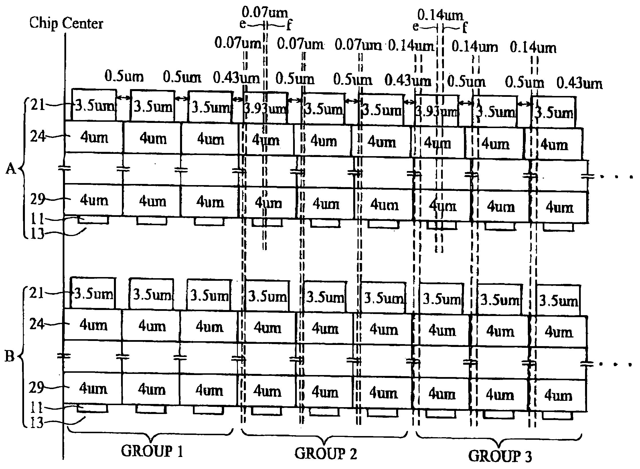
[0023] The present invention provides a method to improve non-uniformly effective incident light and to avoid cross-talk between adjacent pixels in a sensor chip. The microlens layer consists of a plurality of microlenses corresponding to each sensing areas The position of the microlens is a function of distance from the microlens to the chip center. Specitically, the microlens is shifted toward the chip center as the distance between the microlens and the chip center increases. If the microlens is shifted, the corresponding color filter is also shifted to make sure the incident light does not pass through the adjacent color filter.

[0024] A sensor chip with 1284×1028 pixels is given as an example. Each pixel has a width of 4 μm. The chief angle in the edge region furthest away from the chip center is 15° and the furthest microlens needs to be shifted 2.1 μm. The pixels are divided into 31 groups. The relationship between the chief angle and shifting amounts of the microlens and the...


PUM


Abstract

An image sensor improving the uniformity of effective incident light. In one example, the size of microlenses disposed in different regions of the image sensor is changed to balance the brightness in different regions, in which the size of each microlens is a function of the distance between the microlens to the chip center In another example, the distance between the center of the microlens and the center of the corresponding sensing area is changed to balance the brightness in different regions and the corresponding color filters are shifted such that the microlens is overlying a corresponding color filter unit without overlying adjacent regions thereof, in which the distance between the center of the microlens and the center of the corresponding sensing area is a function of the distance between the corresponding sensing area to the chip center.

Description

FIELD OF THE INVENTION [0001] This invention relates generally to image sensors. In particular, it relates to a design for image sensor microlenses to improve uniformity of effective incident light at different regions, DESCRIPTION OF THE RELATED ART [0002] Solid state image sensors are necessary components in many optoelectronic devices, including digital cameras, cellular phones, and toys. Conventional image sensors Include both charge coupled device (CCD) image sensors and complementary metal oxide semiconductor (CMOS) image sensors. The basic technology used to form the CMOS image sensor is common to both types sensors. [0003] The CMOS image sensor comprises a photo detector for detecting light and a logic circuit for converting the detected light into an electric signal representing data regarding the detected light. The fill factor, sometimes referred to as the aperture efficiency, is the ratio of the size of the light-sensitive area to the size of the total pixel size. Althou...

Claims


Application Information

Patent Timeline
Patent Type & Authority Applications(United States)
IPC IPC(8): G02B3/00H01L27/00H01L27/14H01L27/146H04N5/335
CPCH01L27/14621H01L27/14643H01L27/14627
Inventor HSU, HUNG-JENCHANG, CHIU-KUNGHSIUNG, CHUNG-SHENGWONG, FU-TIEN
Owner TAIWAN SEMICON MFG CO LTD
Why Eureka
Try Eureka