Semiconductor device, method for manufacturing the same, circuit board, and electronic apparatus

a semiconductor and semiconductor technology, applied in the direction of semiconductor devices, semiconductor/solid-state device details, electrical apparatus, etc., can solve the problems of reducing yield, reducing productivity, and difficult to handle the thickness of semiconductor wafers, so as to increase productivity and reliability

Active Publication Date: 2005-03-03
ADVANCED INTERCONNECT SYST LTD
View PDF15 Cites 39 Cited by
  • Summary
  • Abstract
  • Description
  • Claims
  • Application Information

AI Technical Summary

Benefits of technology

[0005] An exemplary embodiment of the invention includes a semiconductor device, a method for manufacturing the same, a circuit board and an electronic apparatus with increased productivity and reliability.
[0006] An exemplary method for manufacturing a semiconductor device of the present invention includes: (a) forming a conductive part in a concave part on a first surface of a substrate, the first surface having a plurality of chip mounting areas; (b) stacking a semiconductor chip in the chip mounting areas; (c) providing a sealing member on the first surface of the substrate; and (d) making part of a second surface of the substrate thin so as to make the conductive part penetrate from the first surface to the second surface. In the present invention, the substrate is reinforced by the sealing member. Therefore, it is possible to make the substrate thin in a stable manner enhances and / or improves reliability. Since the substrate has the plurality of chip mounting areas, it is possible to collectively manufacture semiconductor devices having a multiple stack structure, and thereby enhances and / or improves productivity.

Problems solved by technology

This, however, requires handling by the unit of the semiconductor chips throughout a manufacturing process and fails to provide high productivity.
This also involves problems of not only reducing yield, but also making it difficult to handle the semiconductor wafers whose thickness has been reduced.

Method used


Image

  • Semiconductor device, method for manufacturing the same, circuit board, and electronic apparatus
  • Semiconductor device, method for manufacturing the same, circuit board, and electronic apparatus
  • Semiconductor device, method for manufacturing the same, circuit board, and electronic apparatus

Examples


Embodiment Construction

[0040] Exemplary embodiments of the present invention are described below with reference to the accompanying drawings.

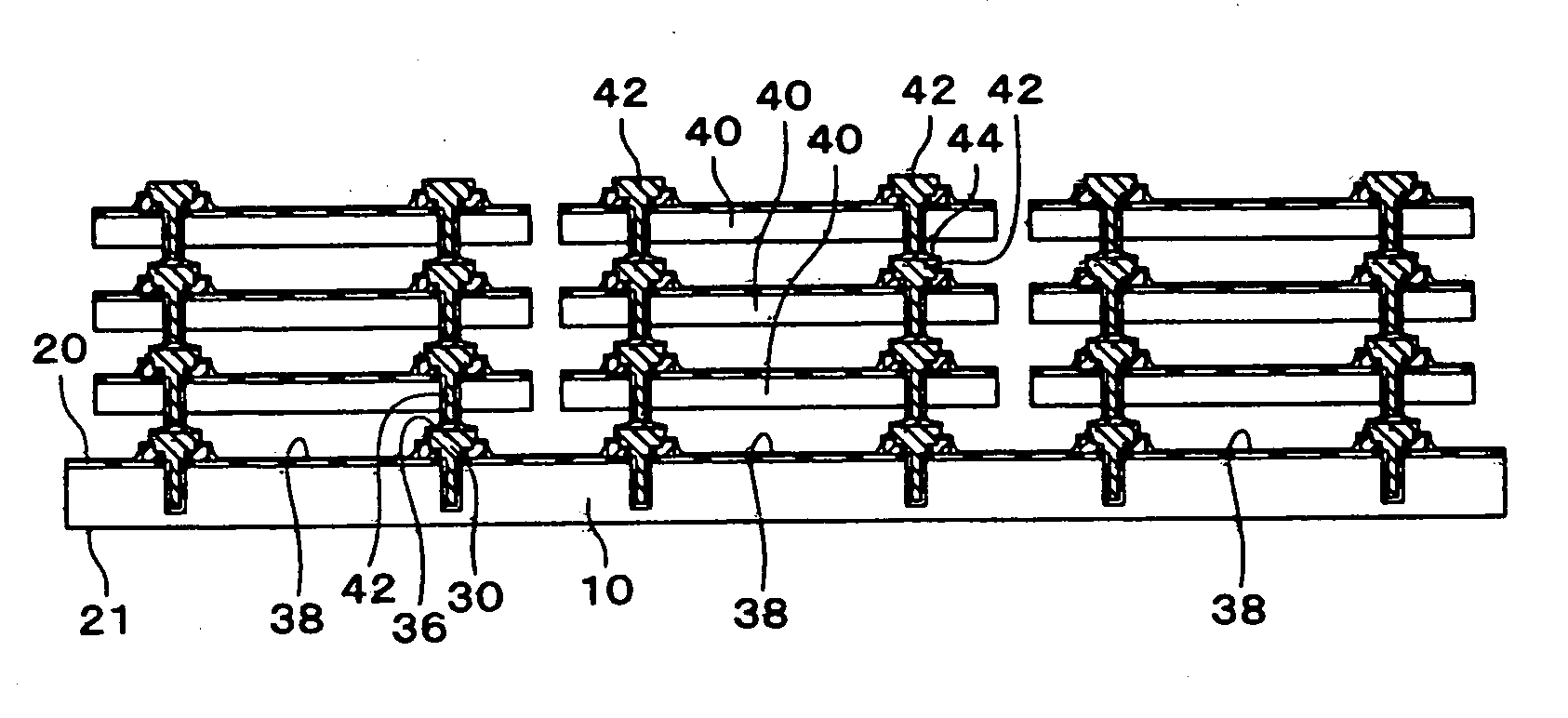
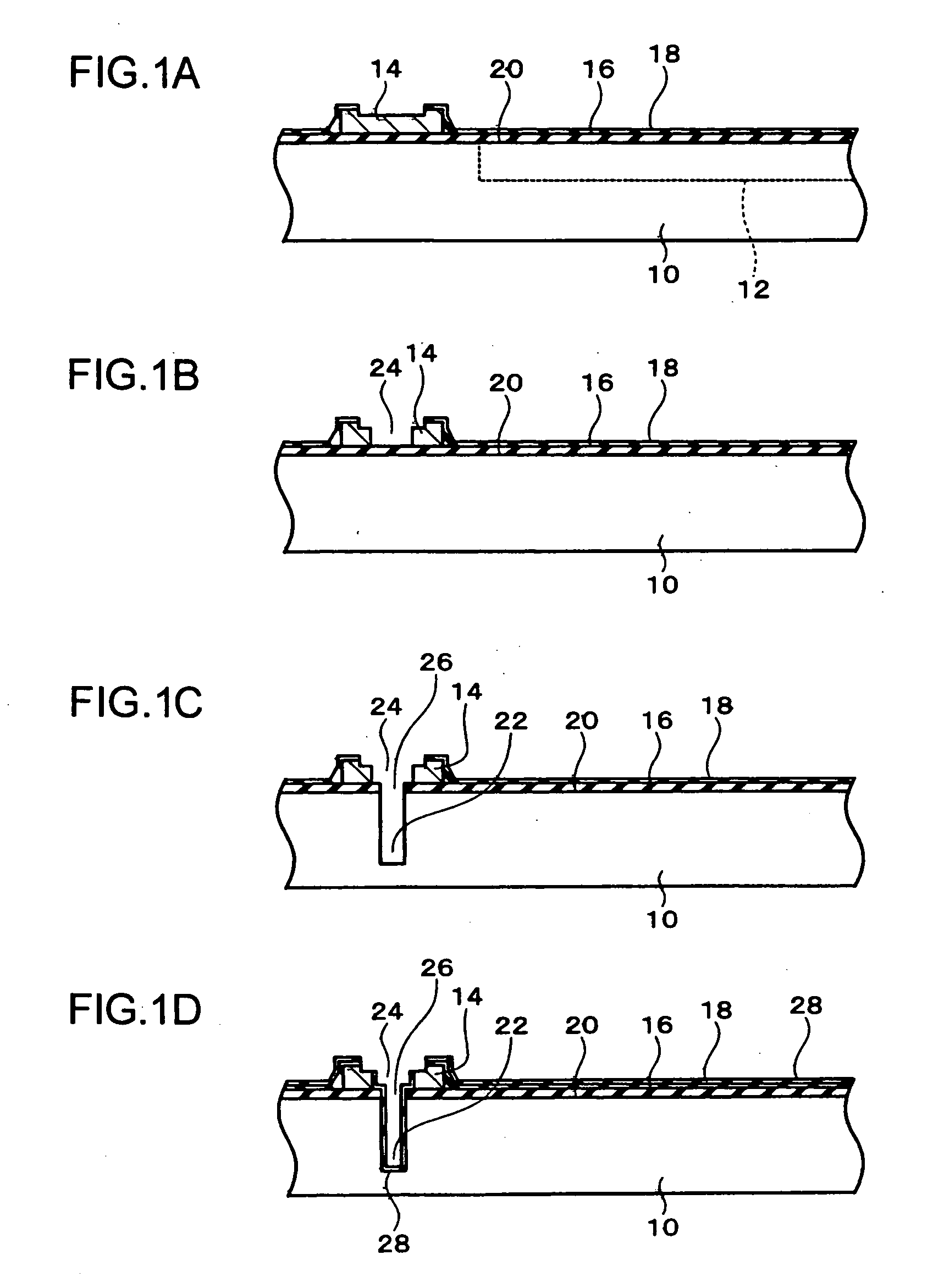
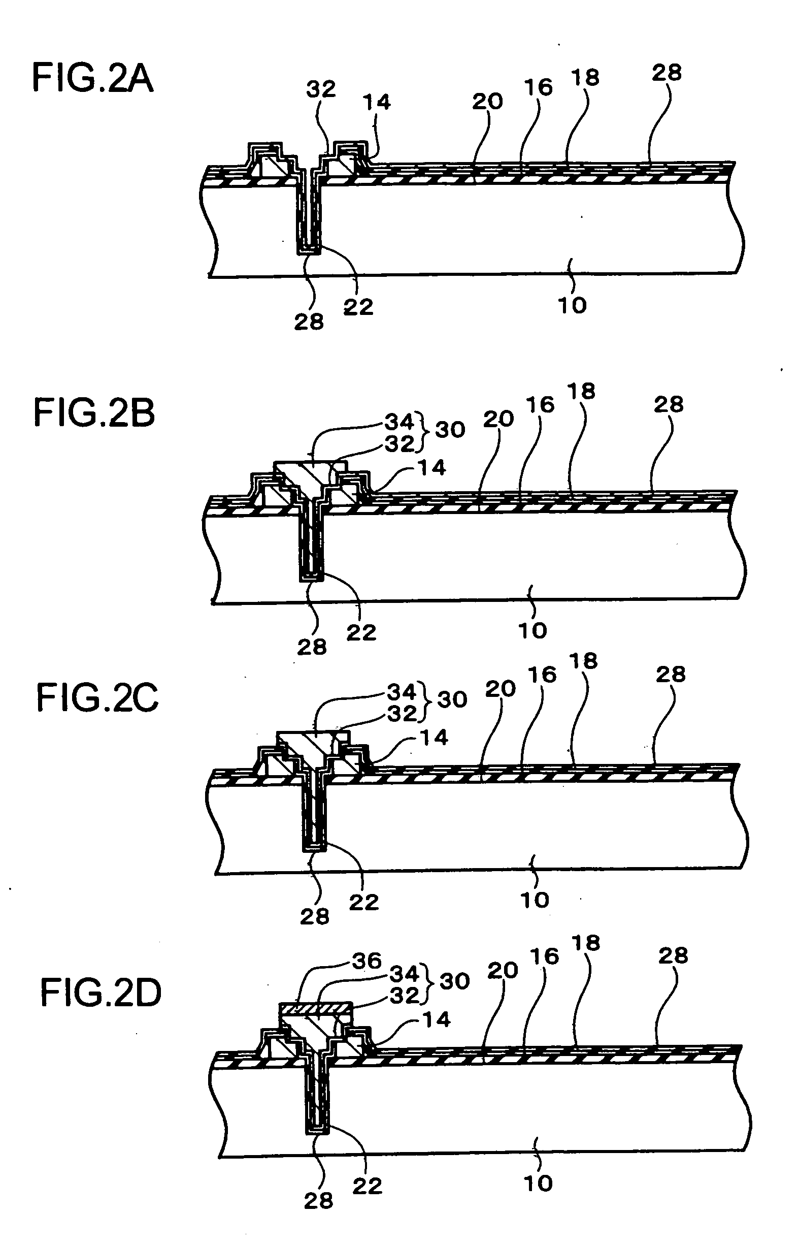
[0041]FIGS. 1A through 8 illustrate a semiconductor device and a method for manufacturing the semiconductor device according to a first exemplary embodiment of the present invention. First, a substrate (semiconductor substrate 10) is prepared. The present embodiment uses the semiconductor substrate (a silicon substrate, for example) 10 as this substrate. The semiconductor substrate 10 may be a semiconductor wafer. In the present exemplary embodiment, an integrated circuit (IC) 12 is provided in the plural number to the semiconductor substrate 10 as shown in FIG. 3A. An electrode (a pad, for example) 14 that is electrically coupled to the IC 12 may be also provided on the semiconductor substrate 10. Multiple electrodes 14 may be provided to each IC 12. The multiple electrodes 14 may be aligned along edges of the IC 12, for example, along two opposing sides or four si...


PUM


Abstract

Exemplary embodiments of the present invention include a semiconductor device, a method for manufacturing the same, a circuit board and an electronic apparatus with increased productivity and reliability. An exemplary method for manufacturing a semiconductor device of the present invention includes forming a conductive part in a concave part on a first surface of a semiconductor substrate, the first surface having a plurality of chip mounting areas. Stacking at least one semiconductor chip in each of the chip mounting areas, providing a sealing member on the first surface of the semiconductor substrate and making part of a second surface of the semiconductor substrate thin so as to make the conductive part penetrate from the first surface to the second surface.

Description

BACKGROUND OF THE INVENTION [0001] 1. Field of Invention [0002] The present invention relates to a semiconductor device, a method for manufacturing the same, a circuit board and an electronic apparatus. [0003] 2. Description of Related Art [0004] Some related art semiconductor devices employ three dimensional packaging technology. One way to reduce the total thickness of such devices is thinly grinding each semiconductor substrate. The related art includes a plurality of semiconductor chips are stacked to form a semiconductor device. This, however, requires handling by the unit of the semiconductor chips throughout a manufacturing process and fails to provide high productivity. Alternatively, a plurality of semiconductor wafers can be stacked and then separated into pieces. This also involves problems of not only reducing yield, but also making it difficult to handle the semiconductor wafers whose thickness has been reduced. The related art also includes a device disclosed in Japane...

Claims


Application Information

Patent Timeline
Patent Type & Authority Applications(United States)
IPC IPC(8): H01L25/18H01L21/768H01L23/31H01L23/48H01L25/065H01L25/07
CPCH01L21/76898H01L2924/01024H01L23/481H01L23/49816H01L24/97H01L25/0657H01L25/50H01L2224/16H01L2224/32145H01L2224/48091H01L2224/73265H01L2224/97H01L2225/0651H01L2225/06513H01L2225/06517H01L2225/06541H01L2225/06586H01L2924/01013H01L2924/01027H01L2924/01029H01L2924/01033H01L2924/01074H01L2924/01078H01L2924/01082H01L2924/14H01L23/3114H01L2924/01006H01L2924/01005H01L24/48H01L2224/85H01L2924/00014H01L2224/81H01L2224/83H01L24/05H01L2224/02377H01L2224/05001H01L2224/05009H01L2224/05124H01L2224/05147H01L2224/05548H01L2224/13025H01L2224/16145H01L2924/12042H01L2924/181H01L2924/00H01L2924/00012H01L2224/45099H01L2224/45015H01L2924/207
Inventor YAMAGUCHI, KOJI
Owner ADVANCED INTERCONNECT SYST LTD
Why Eureka
Try Eureka