Molecularly controlled dual gated field effect transistor for sensing applications

a dual gated field effect transistor and sensing technology, applied in the field of semiconductor devices, can solve the problems of unmatched sensitivity of hybrid organic/inorganic sensors, unfavorable static use, and high noise levels compared to gated devices, and achieve the effect of large detection area and high sensitivity

Inactive Publication Date: 2005-03-10
INTERUNIVERSITAIR MICRO ELECTRONICS CENT (IMEC VZW)
View PDF7 Cites 57 Cited by
  • Summary
  • Abstract
  • Description
  • Claims
  • Application Information

AI Technical Summary

Problems solved by technology

In consideration to their direct and fast transduction principle, hybrid organic / inorganic sensors allow real-time monitoring of dynamic processes with unparalleled sensitivity.
These ungated devices are oversensitive to electrical interferences, which leads to unwanted high noise levels compared to gated devices.
This configuration presents the disadvantage of a static use requiring an adaptation of the thickness for each type detection.
However, being a depletion mode device, it lacks the necessity of actively biasing the transistor into conduction.
Furthermore, when used as described in Perkins, the device becomes sensitive to neutral molecules since their adsorption on the organic sensing layer changes the capacitive coupling of the voltage of the electrolyte solution to the channel, resulting in a mere linear change of the source-drain current.
The consequence is a lower sensitivity due to the inherent native oxide of silicon which implies tight specifications for packaging due to current carrying electrodes at the solution side of the device.

Method used


Image

  • Molecularly controlled dual gated field effect transistor for sensing applications
  • Molecularly controlled dual gated field effect transistor for sensing applications

Examples


Embodiment Construction

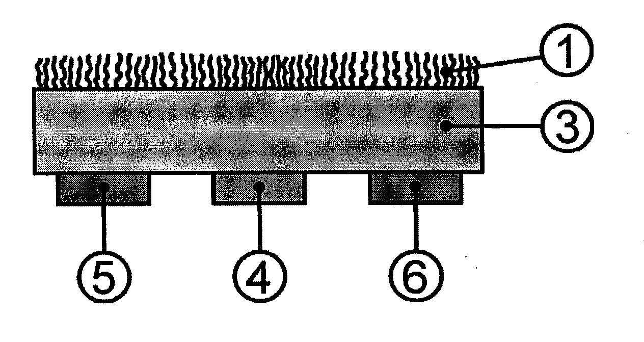
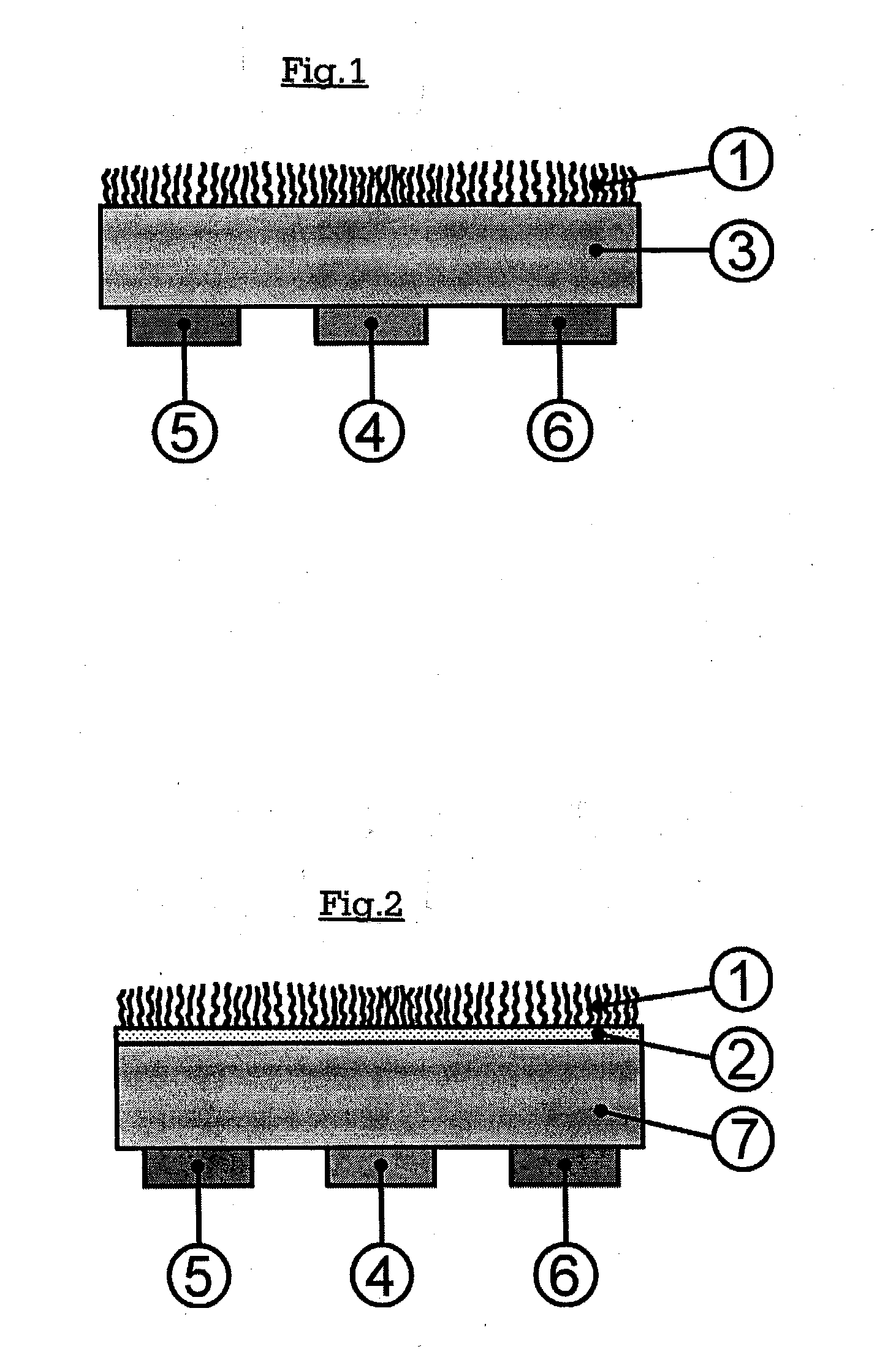
The present invention discloses a sensing device comprising an organic sensing layer (1) having at least one functional group that binds to the semiconductor layer (3) and at least another functional group that serves as a sensor, a semiconductor layer (3) having a first side and a second side, a drain electrode (6), a source electrode (5), a gate electrode (4), wherein said source electrode (5), said drain electrode (6) and said gate electrode (4) are situated on the first side of said semiconductor layer and that said sensing layer (1) is situated on the second side of said semiconductor layer and that said sensing gate layer (1) is operatively associated with the semiconductor layer and that said semiconductor layer has a thickness below 5000 nm.

Said sensing device converts a non-electrical signal into an electrical signal. A non-electrical signal may be generated by a physical or a chemical event. The physical or chemical event may be, but is not limited hereto, a change of t...


PUM

PropertyMeasurementUnit
thicknessaaaaaaaaaa
thicknessaaaaaaaaaa
thicknessaaaaaaaaaa

Abstract

A sensing device and method of making and using the sensing device. The device comprises a sensing gate layer of multifunctional organic sensing molecules having at least one functional group that binds to the semiconductor layer and at least another functional group that serves as a sensor. The device further comprises a semiconductor channel layer, a drain electrode, a source electrode, and a biasing gate. The source and drain electrodes and biasing gate are situated on the same side of the device and simultaneously on the opposite side of the sensing gate layer. The sensing gate layer may be directly in contact with the intermediate layer or the semiconductor channel layer.

Description

FIELD OF THE INVENTION The present invention relates to the field of semiconductor devices and more particularly to hybrid organic / inorganic sensors used for the direct sensing upon double gate transistors. DESCRIPTION OF THE RELATED ART A sensor is a device used to detect ions, molecules or energies of any kind. Its sensitivity and its selectivity as well as the lifetime determine the quality of a sensor. The combination of semiconductors with organic molecules is an attractive option for sensors. This combination offers the advantage to associate sensitivity and selectivity through a molecular detection layer. A mere change in electron density or electronegativity of the molecular surface-adsorbate complex, upon physical or chemical perturbation, results in a direct and fast change of electro-optical properties of the semiconductor sensor. In consideration to their direct and fast transduction principle, hybrid organic / inorganic sensors allow real-time monitoring of dynamic pr...

Claims


Application Information

Patent Timeline
Patent Type & Authority Applications(United States)
IPC IPC(8): G01N27/414
CPCB82Y10/00G01N27/4145B82Y30/00B82Y15/00
Inventor KEERSMAECKER, KOEN DEBORGHS, GUSTAAF
Owner INTERUNIVERSITAIR MICRO ELECTRONICS CENT (IMEC VZW)
Why Eureka
Try Eureka