Fabrication of diaphragms and "floating" regions of single crystal semiconductor for MEMS devices

a technology of semiconductors and diaphragms, applied in the field of microelectromechanical structures, or mems, can solve the problems of low strength of polysilicon and its resistance to crack formation and associated mechanical failure, and achieve the effect of accurate and simple techniqu

Inactive Publication Date: 2005-03-10
JBCR INNOVATIONS
View PDF17 Cites 2 Cited by
  • Summary
  • Abstract
  • Description
  • Claims
  • Application Information

AI Technical Summary

Benefits of technology

[0021] The practice of this invention can also create DMD (Deformed Mirror Device) and air bridge devices with an accurate and simple technique.

Problems solved by technology

The use of polysilicon is sufficient in some applications, but the strength of polysilicon and its resistance to crack formation and associated mechanical failure are not as high as those of single crystal materials.
The ever increasing complexity of integrated devices having greater numbers of wiring channels coupled with the desire for packing chips closer together to minimize transmission delays, results in the need for multilayered and high channel density interconnect substrates.

Method used


Image

  • Fabrication of diaphragms and "floating" regions of single crystal semiconductor for MEMS devices
  • Fabrication of diaphragms and "floating" regions of single crystal semiconductor for MEMS devices
  • Fabrication of diaphragms and "floating" regions of single crystal semiconductor for MEMS devices

Examples


Embodiment Construction

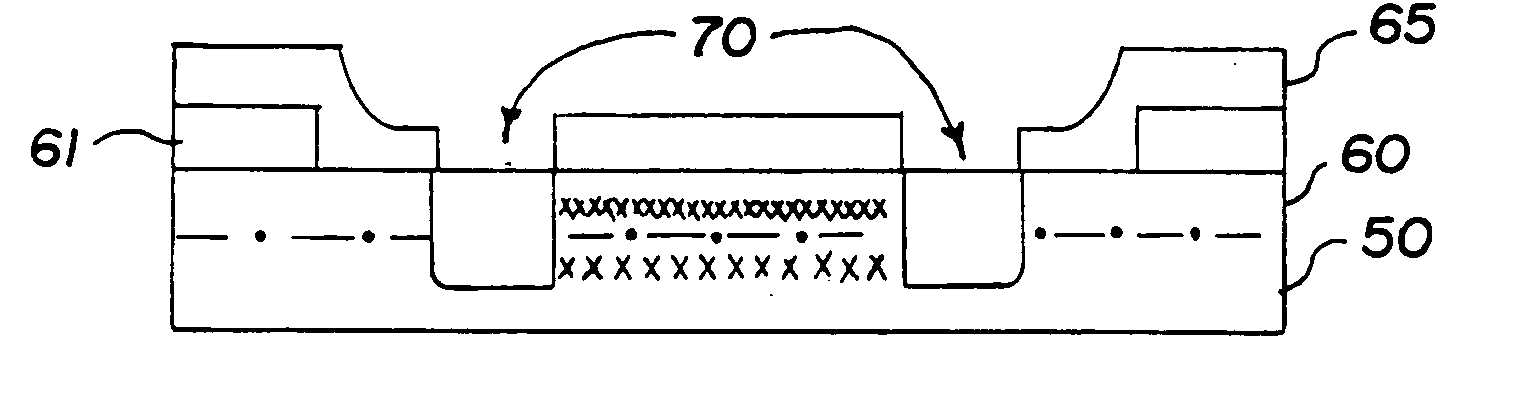
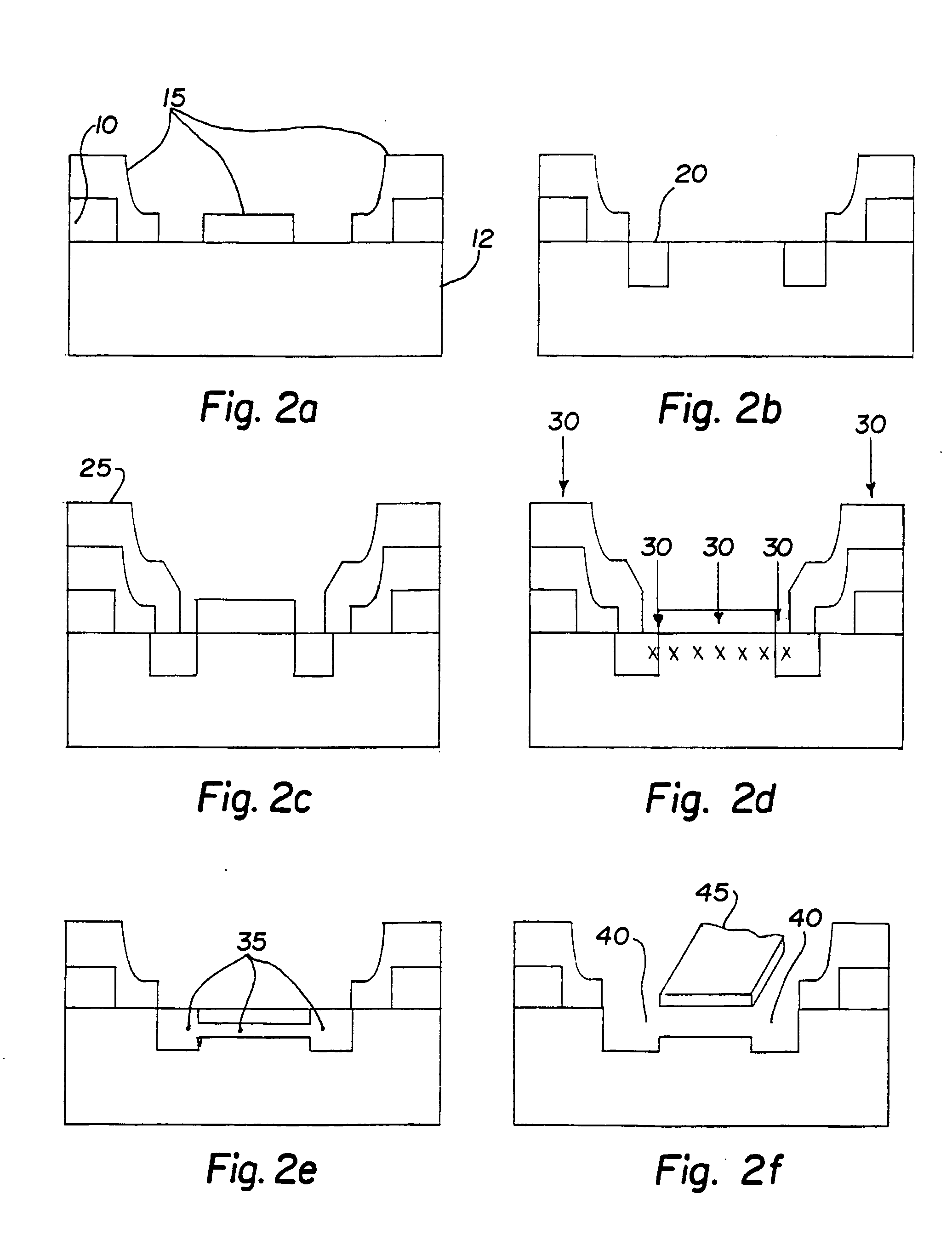
[0029]FIG. 2, to which reference should now be made, illustrates a representation of the sequence of steps used to manufacture microelectromechanical (MEMS) devices with a process that allows the formation of floating or cantilevered single crystal structures instead of the polysilicon structures used in the prior art.

[0030] In FIG. 2a, an etch stop layer 15 such as silicon nitride is deposited over existing structures 11 using a vapor deposition process typically in the temperature range of 800° C.-900° C., and then masked and etched, leaving the nitride in direct contact with the surface of a single crystalline substrate at the boundaries of all regions that will not become floating structures, leaving regions that will become floating structures in between

[0031] In FIG. 2b, using a thermal oxidation furnace in a temperature range of 800° C.-1250° C., perform a local oxidation of silicon (LOCOS) process sequence after a trench etch step. This process sequence can include any of ...


PUM


Abstract

A single crystal semiconductor region is fabricated in a semiconductor wafer. The region is either cantilevered, supported at one or both ends, or midpoint, or supported at multiple locations. After a pattern and etch step, a dielectric fill step is performed to define the boundaries of the region in the semiconductor wafer. Oxygen or nitrogen is implanted in the semiconductor wafer on a surface area of the semiconductor wafer that corresponds to a top surface of the region. The annealing of the oxygen or nitrogen ions convert the silicon to an oxide or a nitride beneath the surface area. The silicon dioxide or silicon nitride is etched away to produce a semiconducting region of a single crystal material.

Description

BACKGROUND OF THE INVENTION [0001] This invention relates to Microelectromechanical Structure, or MEMS, and the method of fabricating such devices. [0002] Microelectromechanical Structures, or “MEMS” often consist in part, of polycrystalline semiconductor regions that are only partially attached to the underlying material. Such polycrystalline silicon regions, which may be cantilevered, center supported or supported at both ends are hereinafter referred to as “regions”. They are typically formed by depositing polysilicon on a layer of sacrificial material such as a silicon nitride, silicon dioxide, or another dielectric. Often the polysilicon material, either doped or undoped as required by the design, is masked and patterned using a photolithographic process to define the desired structure(s). The underlying sacrificial layer is partially or totally removed, leaving the layer of polysilicon material unsupported except at selected support locations. This sequence of steps allows the...

Claims


Application Information

Patent Timeline
Patent Type & Authority Applications(United States)
IPC IPC(8): B81B3/00
CPCB81B3/0035
Inventor BLANCHARD, RICHARD A.
Owner JBCR INNOVATIONS
Why Eureka
Try Eureka