Semiconductor film, method for manufacturing the semiconductor film, solar cell using the semiconductor film and method for manufacturing the solar cell

a semiconductor film and semiconductor technology, applied in the field of semiconductors, can solve the problems of deterioration in conversion efficiency in some cases, increase in crystal defects in some cases, and limit the method of forming a na-containing layer on the control of carrier density, and achieve the effect of effective control

Inactive Publication Date: 2005-03-17
PANASONIC CORP
View PDF2 Cites 25 Cited by
  • Summary
  • Abstract
  • Description
  • Claims
  • Application Information

AI Technical Summary

Benefits of technology

[0007] Therefore, with the foregoing in mind, it is an object of the present invention to provide a semiconductor film whose carrier density is controlled effectively, a method for manufacturing the semiconductor film, a solar cell using the semiconductor film and a method for manufacturing the solar cell.

Problems solved by technology

According to the method of forming a Na-containing layer, followed by the formation of a CIGS film thereon, however, a sufficient increase in carrier density cannot be obtained, which means a low open circuit voltage of a solar cell, thus resulting in a deterioration in the conversion efficiency in some cases.
In the case where the doping amount of Na is increased by increasing a film thickness of the Na-containing layer, the crystal growth of the CIGS film is inhibited, which results in an increase in crystal defects in some cases.
In this way, the method of forming a Na-containing layer has a limit on the control of the carrier density.
In this case, there is a problem that the carrier density does not increase in proportion to the doped amount, and therefore there still is a limit on the control of the carrier density.

Method used


Image

  • Semiconductor film, method for manufacturing the semiconductor film, solar cell using the semiconductor film and method for manufacturing the solar cell
  • Semiconductor film, method for manufacturing the semiconductor film, solar cell using the semiconductor film and method for manufacturing the solar cell
  • Semiconductor film, method for manufacturing the semiconductor film, solar cell using the semiconductor film and method for manufacturing the solar cell

Examples


embodiment 1

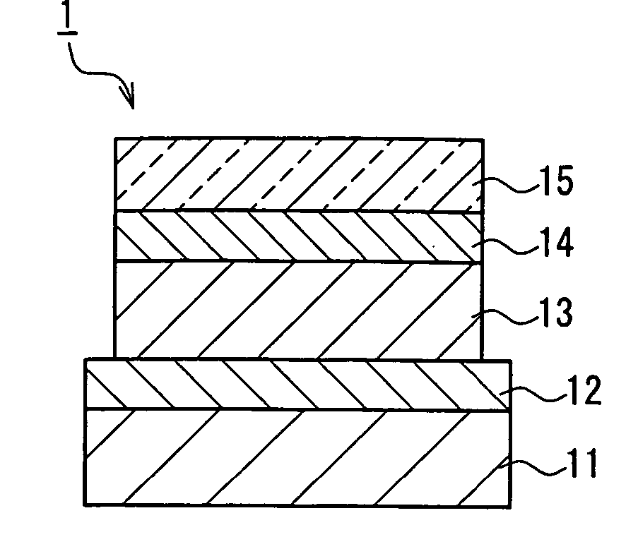
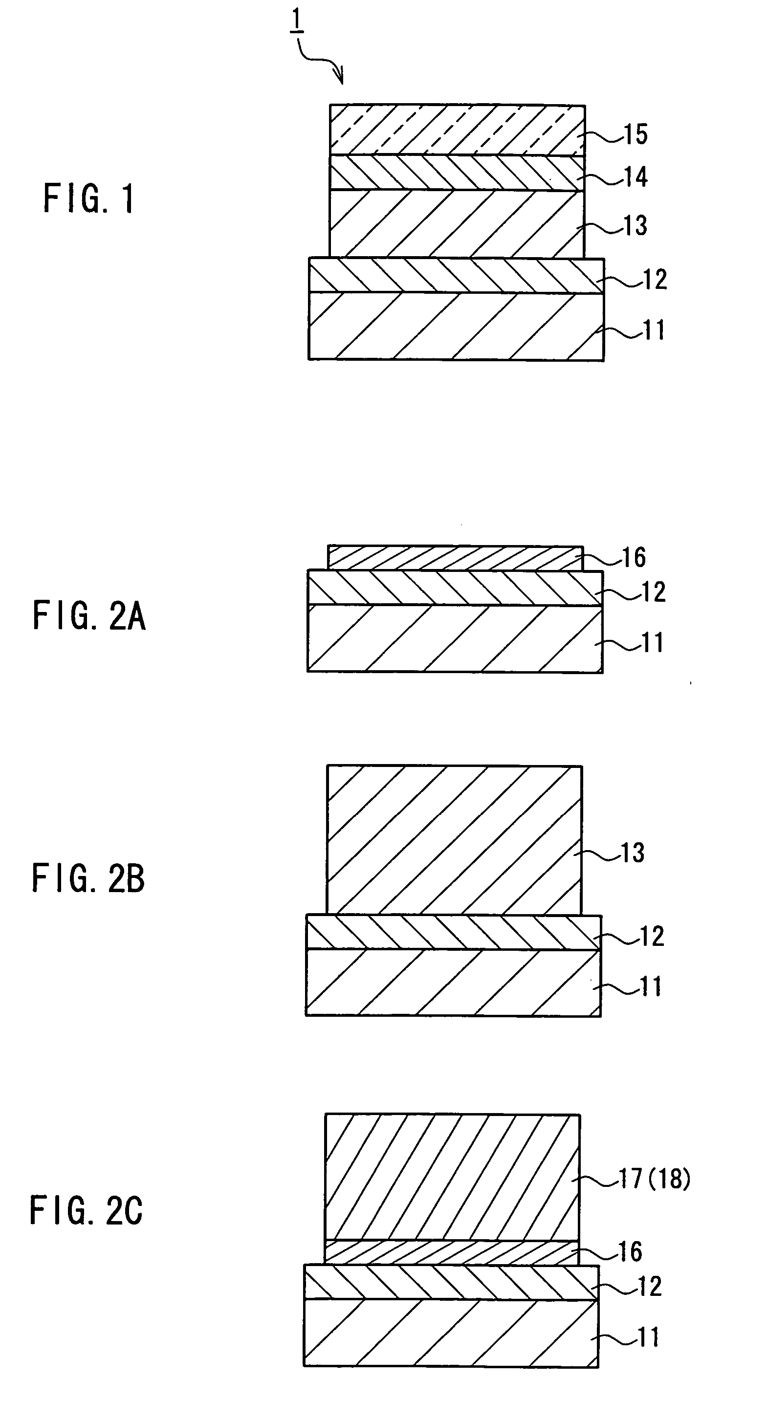
[0052]FIG. 1 is a cross-sectional view showing one embodiment of a solar cell of the present invention. As shown in FIG. 1, a solar cell 1 of the present embodiment is formed to include an electrode layer 12, a light-absorption layer 13, a window layer 14 and a transparent electrode layer 15 that are laminated in this stated order on a substrate 11.

[0053] As the substrate 11, a glass substrate, a metal substrate (stainless steel board, Ti board and the like) or a metal substrate coated with an insulation film can be used, for example.

[0054] The electrode layer 12 is formed of, for example, a metal thin film such as Mo.

[0055] As the window layer 14, Zn based compounds such as ZnO and Zn1-xMgxO (02O3 and In2S3 or oxides such as Ga2O3 and Al2O3 can be used, for example.

[0056] As the transparent electrode layer 15, ITO and ZnO:Al or ZnO:Ga in which a Group III element such as Al or Ga is doped to ZnO, etc., can be used, for example.

[0057] The light-absorption layer 13 is a semicond...

embodiment 2

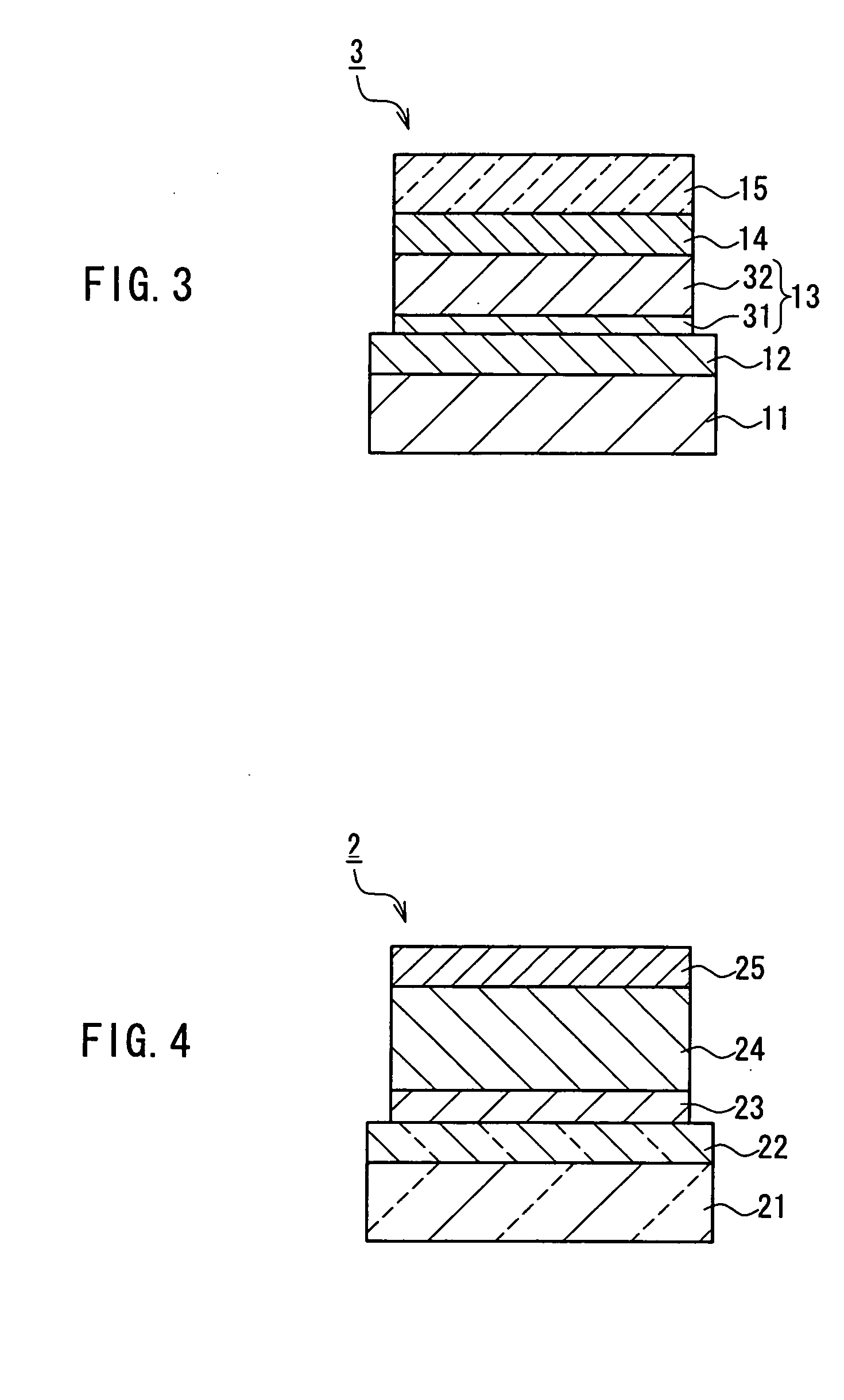
[0066]FIG. 4 is a cross-sectional view showing another embodiment of a solar cell of the present invention. As shown in FIG. 4, a solar cell2 of the present embodiment is formed to include a transparent electrode layer 22, a window layer 23, a light-absorption layer 24 and an electrode layer 25 that are laminated in this stated order on a transparent substrate 21.

[0067] As the transparent substrate 21, a glass substrate can be used, for example.

[0068] As the transparent electrode layer 22, ITO and ZnO:Al or ZnO:Ga in which a Group III element such as Al or Ga is doped to ZnO, etc., can be used, for example.

[0069] As the window layer 23, Zn based compounds such as ZnO and Zn1-xMgxO (02O3 and In2S3 or oxides such as Ga2O3 and Al2O3 can be used, for example.

[0070] The light-absorption layer 24 is a semiconductor layer (semiconductor film) formed of the same materials and with the same manufacturing method as those of the light-absorption layer 13 described in Embodiment 1. Similarl...

embodiment 3

[0077] The following describes still another embodiment of the method for manufacturing a solar cell of the present invention. The manufacturing method of the present embodiment is different from the manufacturing methods described in Embodiment 1 and Embodiment 2 in the steps for manufacturing the light-absorption layers 13 and 24 of the solar cells 1 and 2 shown in FIGS. 1 and 4. According to the manufacturing method of the present embodiment, when a Group Ib element, a Group IIIb element and a Group VIb element are supplied, a Group Ia element and a Group Vb element also are supplied concurrently so as to form a semiconductor layer functioning as the light-absorption layers 13 and 24.

[0078] As the Group Ib element, the Group IIIb element and the Group VIb element, the Group Ia element and the Group Vb element, the same materials as those described in Embodiment 1 may be used, for example. As a method for supplying the Group Ib element, the Group IIIb element and the Group VIb el...


PUM


Abstract

A semiconductor film has a composition in which a Group Ia element and a Group Vb element are added to a compound semiconductor with a chalcopyrite structure containing a Group Ib element, a Group IIIb element and a Group VIb element. This allows the provision of a semiconductor film whose carrier density can be controlled effectively. A solar cell of the present invention includes: a substrate and the semiconductor film of the present invention that is provided as a light-absorption layer on the substrate. With this configuration, a light-absorption layer whose carrier density can be controlled effectively can be provided, so that a solar cell having a high energy conversion efficiency can be provided.

Description

FIELD OF THE INVENTION [0001] The present invention relates to a semiconductor film, a method for manufacturing the semiconductor film, a solar cell using the semiconductor film and a method for manufacturing the solar cell. BACKGROUND OF THE INVENTION [0002] Solar cells using CuInSe2 (hereinafter referred to as CIS) and Cu(In, Ga)Se2 (hereinafter referred to as CIGS) as a light-absorption layer have an advantage of showing a high energy conversion efficiency and being free from a deterioration in the efficiency caused by the irradiation with light, where the CuInSe2 is a compound semiconductor (chalcopyrite structured semiconductor) containing a Group Ib element, a Group IIIb element and a Group VIb element and the Cu(In, Ga)Se2 is a solid solution of CIS with Ga. [0003] Generally speaking, in order to enhance the efficiency of a solar cell, it is important to control the carrier density. For instance, it is known that, in a solar cell using a CIGS film that is a semiconductor film...

Claims


Application Information

Patent Timeline
Patent Type & Authority Applications(United States)
IPC IPC(8): G02B15/14H01L29/732H01L31/00H01L31/0264H01L31/0288H01L31/032H01L31/0328H01L31/0336H01L31/042H01L31/072H01L31/109H01L31/18
CPCH01L31/0323Y02E10/541Y02E10/52Y02P70/50
Inventor NEGAMI, TAKAYUKISATOH, TAKUYAHASHIMOTO, YASUHIRO
Owner PANASONIC CORP
Why Eureka
Try Eureka