Green organic light-emitting diodes

a light-emitting diode and organic technology, applied in the field of organic electroluminescent devices, can solve the problems of insufficient stability of quinacridone derivatives as taught in the prior art, a barrier to many desirable applications, and a performance limitation that is not suitable for many desirable applications

Inactive Publication Date: 2005-03-17
EASTMAN KODAK CO
View PDF4 Cites 44 Cited by
  • Summary
  • Abstract
  • Description
  • Claims
  • Application Information

AI Technical Summary

Benefits of technology

The invention provides an electroluminescent device having a cathode and an anode, an organic light emitting layer (LEL) containing at least one organic host material and a light emitting first dopant, and a layer containing a stabilizing second dopant wherein: a) the organic host material is capable of sustaining both hole and electron injection and recombination of electrons and holes; and b) the first dopant is a green light emitting organic material capable of accepting energy from the electron-hole recombination in the host material and of accepting energy tr

Problems solved by technology

While organic electroluminescent (EL) devices have been known for over two decades, their performance limitations have represented a barrier to many desirable appl

Method used


Image

  • Green organic light-emitting diodes
  • Green organic light-emitting diodes
  • Green organic light-emitting diodes

Examples


examples

The invention and its advantages are further illustrated by the specific examples that follow.

Examples 1, 5, 9, 13, 18, 23

Comparative EL Devices

Comparative EL devices not satisfying the requirements of the invention were constructed in the following manner:

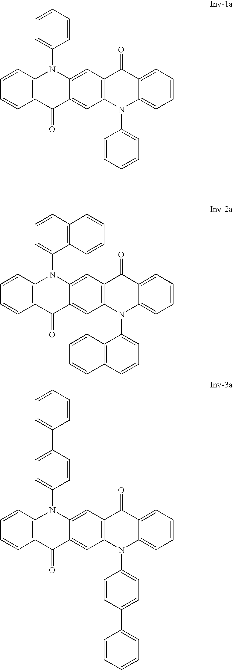
A glass substrate coated with a 42 nm layer of indium-tin oxide (ITO) as the anode was sequentially ultrasonicated in a commercial detergent, rinsed in deionized water, degreased in toluene vapor and exposed to oxygen plasma for about 1 min. a) Over the ITO was deposited a 1 nm fluorocarbon hole-injecting layer (CFx) by plasma-assisted deposition of CHF3. b) A hole-transporting layer of N,N′-di-1-naphthalenyl-N,N′-diphenyl-4,4′-diaminobiphenyl (NPB) having a thickness of 75 nm was then evaporated from a tantalum boat. c) A 37.5 nm light-emitting layer of Alq doped with a first dopant from the “Inv-a” category, in an amount ranging from 0.25% to 2% was then deposited onto the hole-transporting layer. These materials were ...

examples 2-4 , 6-8 , 10-12 , 14-17 , 19-22 , 24-27

Examples 2-4, 6-8, 10-12, 14-17, 19-22, 24-27

Inventive EL Devices

EL inventive devices were fabricated in the same manner as described above except that, the Alq emitting layer is doped with a combination of two dopants (the emitting “Inv-a” first dopant and the stabilizing “Inv-b” second dopant), one from each category Inv-a and Inv-b. The exact dopant percentages used are reported in Tables 1-6.

The cells thus formed in Examples 1-27 were tested for efficiency in the form of luminance yield (cd / A) measured at 20 mA / cm2. CIE color x and y coordinates were determined. It is desirable to have a luminance yield of at least about 7 cd / A and preferably greater than about 8 cd / A. An acceptable green for a high quality full color display device has CIEx of no more than about 0.35 and CIEy no less than about 0.62. The luminance loss was measured by subjecting the cells to a constant current density of 20 mA / cm2 at 25° C. / 70° C., for various amounts of time that are specified for each ind...


PUM

PropertyMeasurementUnit
Fractionaaaaaaaaaa
Nanoscale particle sizeaaaaaaaaaa

Abstract

Disclosed is an electroluminescent device having a cathode and an anode, an organic light emitting layer (LEL) containing at least one organic host material and a light emitting first dopant, and a layer containing a stabilizing second dopant wherein: a) the organic host material is capable of sustaining both hole and electron injection and recombination of electrons and holes; and b) the first dopant is a green light emitting organic material capable of accepting energy from the electron-hole recombination in the host material and of accepting energy transferred from the second dopant and is selected to have a bandgap energy lower than or equal to the bandgap energy of the second dopant material; c) the second dopant is a stabilizing material capable of accepting energy of electron-hole recombination in the host material, the second dopant being selected to have a bandgap energy lower than the bandgap energy of the host material, but higher or equal to the first dopant; wherein emissions from the first dopant and emissions from the second dopant, if any, have a peak emission in the OLED device less than 570 nm.

Description

FIELD OF THE INVENTION This invention relates to organic electroluminescent (EL) devices. More specifically, this invention relates to green EL devices having an emission peak less than 570 nm and containing a selected combination of dopants including a stabilizing dopant. BACKGROUND OF THE INVENTION While organic electroluminescent (EL) devices have been known for over two decades, their performance limitations have represented a barrier to many desirable applications. In simplest form, an organic EL device is comprised of an anode for hole injection, a cathode for electron injection, and an organic medium sandwiched between these electrodes to support charge recombination that yields emission of light. These devices are also commonly referred to as organic light-emitting diodes, or OLEDs. Representative of earlier organic EL devices are Gurnee et al. U.S. Pat. No. 3,172,862, issued Mar. 9, 1965; Gurnee U.S. Pat. No. 3,173,050, issued Mar. 9, 1965; Dresner, “Double Injection Elec...

Claims


Application Information

Patent Timeline
IPC IPC(8): C07C15/28C07C15/38C09K11/06H01L51/00H01L51/30H01L51/40H01L51/50H05B33/14
CPCC07C15/28H05B33/14C09K11/06C09K2211/1003C09K2211/1007C09K2211/1011C09K2211/1029C09K2211/1033C09K2211/1037C09K2211/1044C09K2211/1055C09K2211/107C09K2211/1092H01L51/002H01L51/0054H01L51/0058H01L51/0059H01L51/0067H01L51/0068H01L51/0073H01L51/008H01L51/0084H01L51/0085H01L51/0089H01L51/5012H01L51/5036C07C15/38H10K71/30H10K85/622H10K85/655H10K85/631H10K85/626H10K85/654H10K85/6574H10K85/322H10K85/341H10K85/351H10K85/342H10K50/125H10K50/11
Inventor COSIMBESCU, LELIAHATWAR, TUKARAM K.
Owner EASTMAN KODAK CO
Why Eureka
Try Eureka