Manufacturing method for a power device having an auto-aligned double thickness gate layer and corresponding device

a technology of auto-alignment and dielectric layer, which is applied in the manufacturing of semiconductor/solid-state devices, basic electric elements, electric devices, etc., can solve the problems of low transistor device performance, and achieve the effects of low manufacturing cost, high tolerance, and fast switching

Active Publication Date: 2005-03-17
STMICROELECTRONICS SRL
View PDF7 Cites 3 Cited by
  • Summary
  • Abstract
  • Description
  • Claims
  • Application Information

AI Technical Summary

Benefits of technology

[0013] One embodiment of the present invention provides a power device having a fast switching and a high tolerance to the trigger of gate dielectric layer hard breakdown mechanisms, this device being manufactured with the lowest number of process steps and having such structural and functional features as to allow a very compact device to be obtained, overcoming the limits and drawbacks still affecting prior art devices.

Problems solved by technology

In terms of switching speed, in fact, the reduction of the gate dielectric layer thickness, together with the increase in the gate electrode area being intrinsic in the higher integration density, involves lower transistor device performances because of the increased input and transition capacitive components.
Although advantageous in many aspects, this first solution has several drawbacks connected to the use of alternative materials whose use at industrial level involves long implementation steps being subject to tests which might require prohibitive times for the present market of the devices concerned.

Method used


Image

  • Manufacturing method for a power device having an auto-aligned double thickness gate layer and corresponding device
  • Manufacturing method for a power device having an auto-aligned double thickness gate layer and corresponding device
  • Manufacturing method for a power device having an auto-aligned double thickness gate layer and corresponding device

Examples


second embodiment

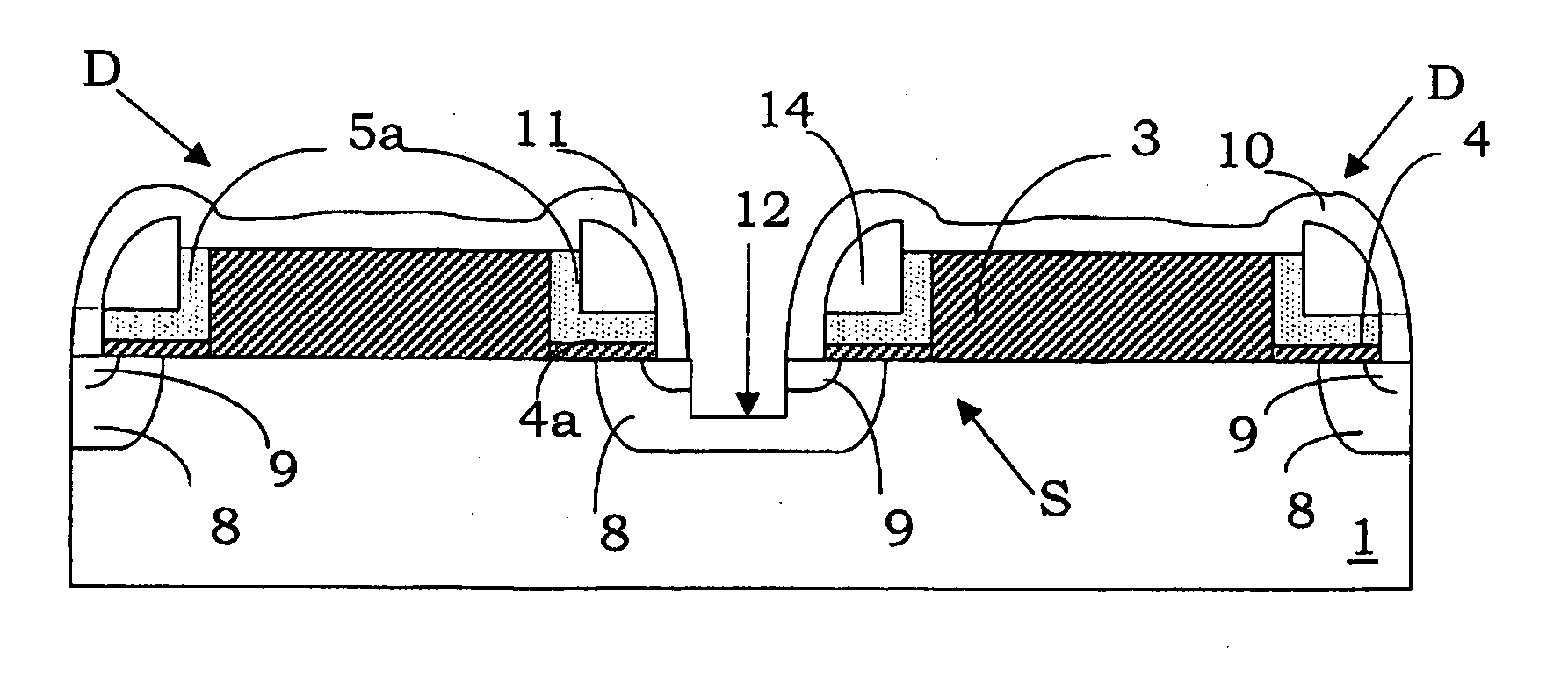
[0030] With reference to FIG. 11, the device D according to the invention is described.

[0031] In this embodiment, the gate electrode 5a is not present on the upper surface of the first dielectric portion 3, but it is present only on the side walls of this first dielectric portion 3.

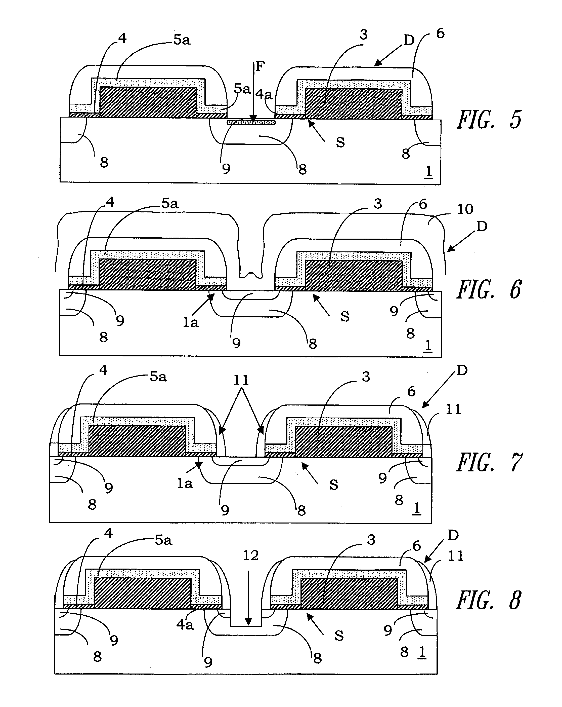
[0032] First spacers 14 are then formed on the gate electrode 5a, as shown in FIG. 10. The device D is then completed by second spacers 11 formed on the side walls of the electrode 5a and they cover at least partially the first spacers 14. These second spacers 11 are formed in a dielectric layer 10 covering the top of both the gate electrode 5a and the first dielectric portions 3.

[0033] In this embodiment too, advantageously, a soft trench 12 is formed in the substrate 1 aligned with the second spacers 11.

first embodiment

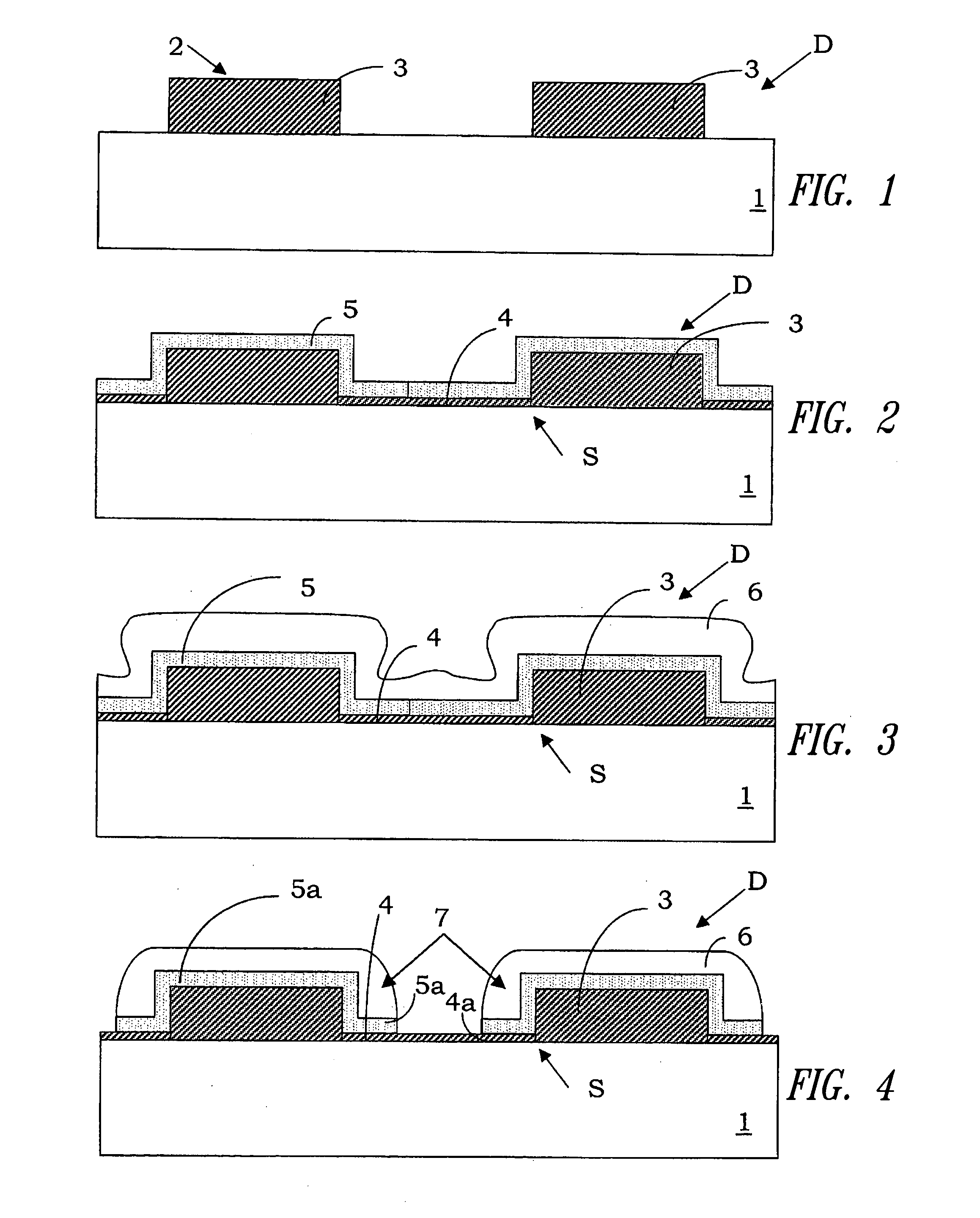
[0034] the manufacturing method of the device D according to the invention is now described.

[0035] Convenient edge terminals, not shown in the figures, are traditionally formed on a semiconductor substrate 1.

[0036] A thin dielectric layer, for example, thermal oxide with a thickness being lower or equal to 100 nm, can be formed on the semiconductor substrate 1, not shown in the figures.

[0037] According to the invention, a thick gate dielectric layer 2 is formed on the substrate 1, for example through CVD (Chemical Vapor Deposition) deposition. (See, FIG. 1)

[0038] The thick dielectric layer 2 is for example a USG (Undoped Silicon Glass), PSG (Phospho-Silicate Glass), BPSG (Boro-Phospho-Silicate Glass), TEOS (Tetraethyl Orthosilicate), SOG (Spin on Glass), silicon nitride layer, or a multilayer comprising a sequence of these layers.

[0039] Advantageously, the thickness of this dielectric layer 2 ranges from 100 to 1000 nm.

[0040] A thermal densifying process of the thick dielectric...


PUM


Abstract

A manufacturing method for a power device integrated on a semiconductor substrate with double thickness of a gate dielectric layer is described, which comprises the following steps: forming first dielectric portions having a first thickness; forming on the whole semiconductor substrate a first dielectric layer thinner than the first dielectric portions; forming a conductive layer on the first dielectric layer; forming a second dielectric layer on the conductive layer; performing an etching step of the second dielectric layer and of the conductive layer to form first spacers and a gate electrode, to define, between the gate electrode and the substrate, second dielectric portions in the first dielectric layer, the second dielectric portions being auto-aligned with the first portions.

Description

BACKGROUND OF THE INVENTION [0001] 1. Field of the Invention [0002] The present invention relates to a manufacturing method for a power device having an auto-aligned double thickness gate dielectric layer and corresponding device. [0003] The invention also relates to a power device integrated on a semiconductor substrate comprising a gate electrode formed above a channel region formed in said semiconductor substrate and insulated therefrom by means of a gate dielectric layer. [0004] The invention particularly, but not exclusively, relates to a manufacturing method of a VDMOS power device and the following description is made with reference to this field of application for convenience of illustration only. [0005] 2. Description of the Related Art [0006] As it is well known, the planar and vertical size decrease and the subsequent power device integration density increase involves the need to reduce the driving potentials of these devices in order to save the strength and integrity th...

Claims


Application Information

Patent Timeline
Patent Type & Authority Applications(United States)
IPC IPC(8): H01L21/336H01L29/423H01L29/78
CPCH01L29/41766H01L29/42368H01L29/7802H01L29/6656H01L29/66712H01L29/42376
Inventor CURRO, GIUSEPPE
Owner STMICROELECTRONICS SRL
Why Eureka
Try Eureka