Method of manufacturing Er-doped silicon nano-dot array and laser ablation apparatus used therein

a technology of laser ablation and erdoped silicon nano-dot array, which is applied in the direction of semiconductor lasers, crystal growth processes, vacuum evaporation coating, etc., can solve the problems of impurities that may occur due to sintering, and achieve high purity and high efficiency

Inactive Publication Date: 2005-03-24
HA JEONG SOOK +3
View PDF14 Cites 5 Cited by
  • Summary
  • Abstract
  • Description
  • Claims
  • Application Information

AI Technical Summary

Benefits of technology

[0009] To solve the above-described problems, it is a first objective of the present invention to provide a method of manufacturing Er-doped silicon arrays by which an Er-doped silicon film having a high purity can be manufactured by preventing contamination due to impurities and the Er-doped silicon film can be patterned as uniformly arrayed Er-doped silicon structures having a nanometer size.
[0025] According to the present invention, an Er-doped silicon thin film having a high efficiency and a high purity can be manufactured in an ultrahigh vacuum. As a result, the Er-doped silicon thin film can be applied in the manufacture of a silicon nano optoelectronic device using silicon as an optoelectronic material. Thus, Er-doped silicon nano-dot arrays can be manufactured using the regular array of copolymers and the selective etching.

Problems solved by technology

Here, impurities may occur due to the sintering.

Method used


Image

  • Method of manufacturing Er-doped silicon nano-dot array and laser ablation apparatus used therein
  • Method of manufacturing Er-doped silicon nano-dot array and laser ablation apparatus used therein
  • Method of manufacturing Er-doped silicon nano-dot array and laser ablation apparatus used therein

Examples


Embodiment Construction

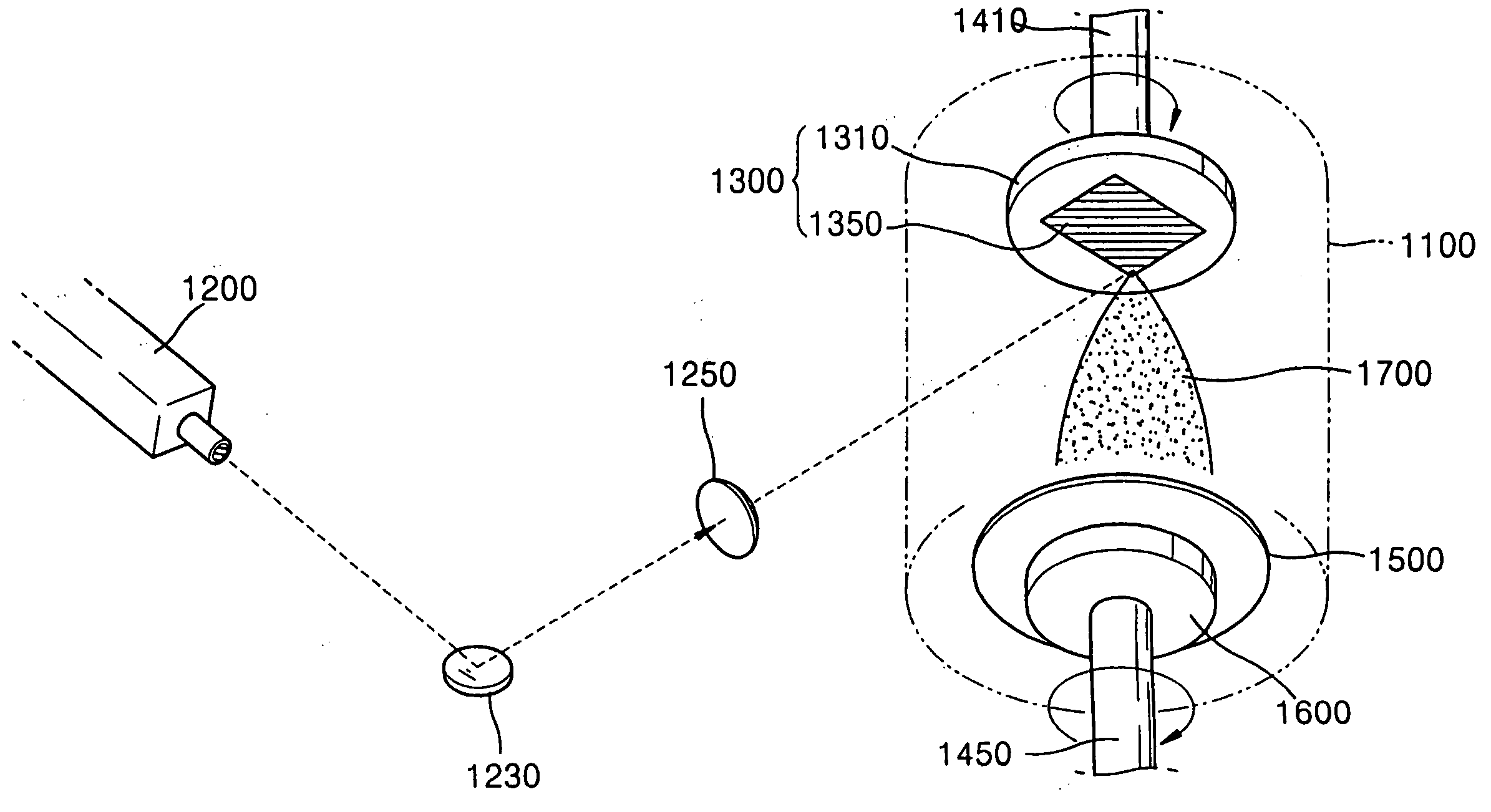
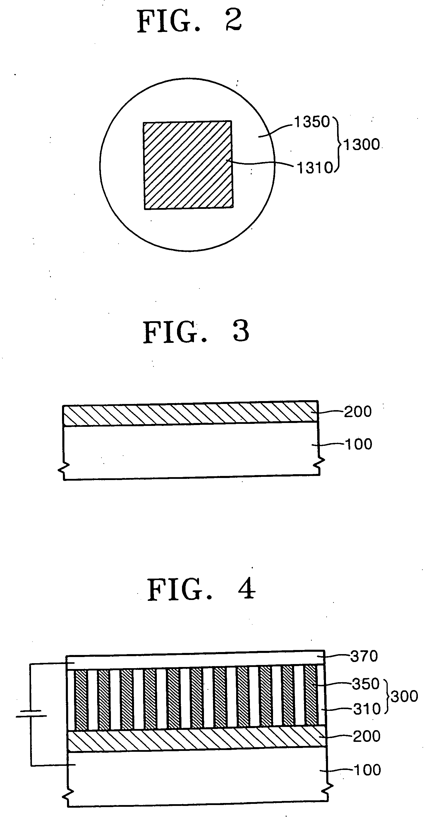
[0030] Hereinafter, embodiments of the present invention will be described in detail with reference to the attached drawings. However, the embodiments of the present invention can be modified into various other forms, and the scope of the present invention must not be interpreted as being restricted to the embodiments. The embodiments are provided to more completely explain the present invention to those skilled in the art. In drawings the thicknesses of layers or regions are exaggerated for clarity. Like reference numerals in the drawings denote the same members. Also, when it is written that a layer is formed “on” another layer or a substrate, the layer can be formed directly on the other layer or the substrate or other layers can intervene therebetween.

[0031] In an embodiment of the present invention, an Er-doped silicon thin film can be prevented from being contaminated due to impurities when the Er-doped silicon thin film is deposited. Thus, a laser ablation method using a new...


PUM

PropertyMeasurementUnit
thicknessaaaaaaaaaa
glass transition temperatureaaaaaaaaaa

Abstract

A laser ablation apparatus. A target has a silicon region and an erbium region divided in a chamber with a silicon substrate opposite to the target. A target rotating axis rotates the target to alternately radiate laser light onto the silicon region and the erbium region, a laser generator irradiates laser light for generating a plume by ablating silicon from the silicon region and erbium from the erbium region outside the chamber.

Description

BACKGROUND OF THE INVENTION [0001] 1. Field of the Invention [0002] The present invention relates to an optoelectronic device, and more particularly, to a method of manufacturing an Er-doped silicon nano-dot array applicable to a silicon optoelectronic device and a laser ablation apparatus used therein. [0003] 2. Description of the Related Art [0004] In order to use silicon having an indirect energy band gap as a material of an optoelectronic device, the development of an efficient method of doping silicon with a luminous substance is required. Also, the development of a method of forming nanometer level silicon structure is required. [0005] Erbium (Er) is treated as a luminous material, which will be doped on silicon. Er-doped silicon has a photoluminescenec (PL) peak of 1.54 μm and thus is noticed in view of a silicon-based optoelectronic device. To manufacture an optoelectronic device using Er-doped silicon, a method of manufacturing a silicon film, which is effectively doped wit...

Claims


Application Information

Patent Timeline
Patent Type & Authority Applications(United States)
IPC IPC(8): C23C14/16C23C14/28H01L21/203
CPCB82Y20/00Y10T117/10C23C14/28C23C14/16B82Y40/00
Inventor HA, JEONG-SOOKPARK, KYOUNG-WANPARK, SEUNG-MINPARK, JONG-HYURK
Owner HA JEONG SOOK
Why Eureka
Try Eureka