Substrate processing apparatus
- Summary
- Abstract
- Description
- Claims
- Application Information
AI Technical Summary
Benefits of technology
Problems solved by technology
Method used
Image
Examples
Embodiment Construction
[0044] A preferred embodiment according to the present invention will now be described in detail with reference to the drawings.
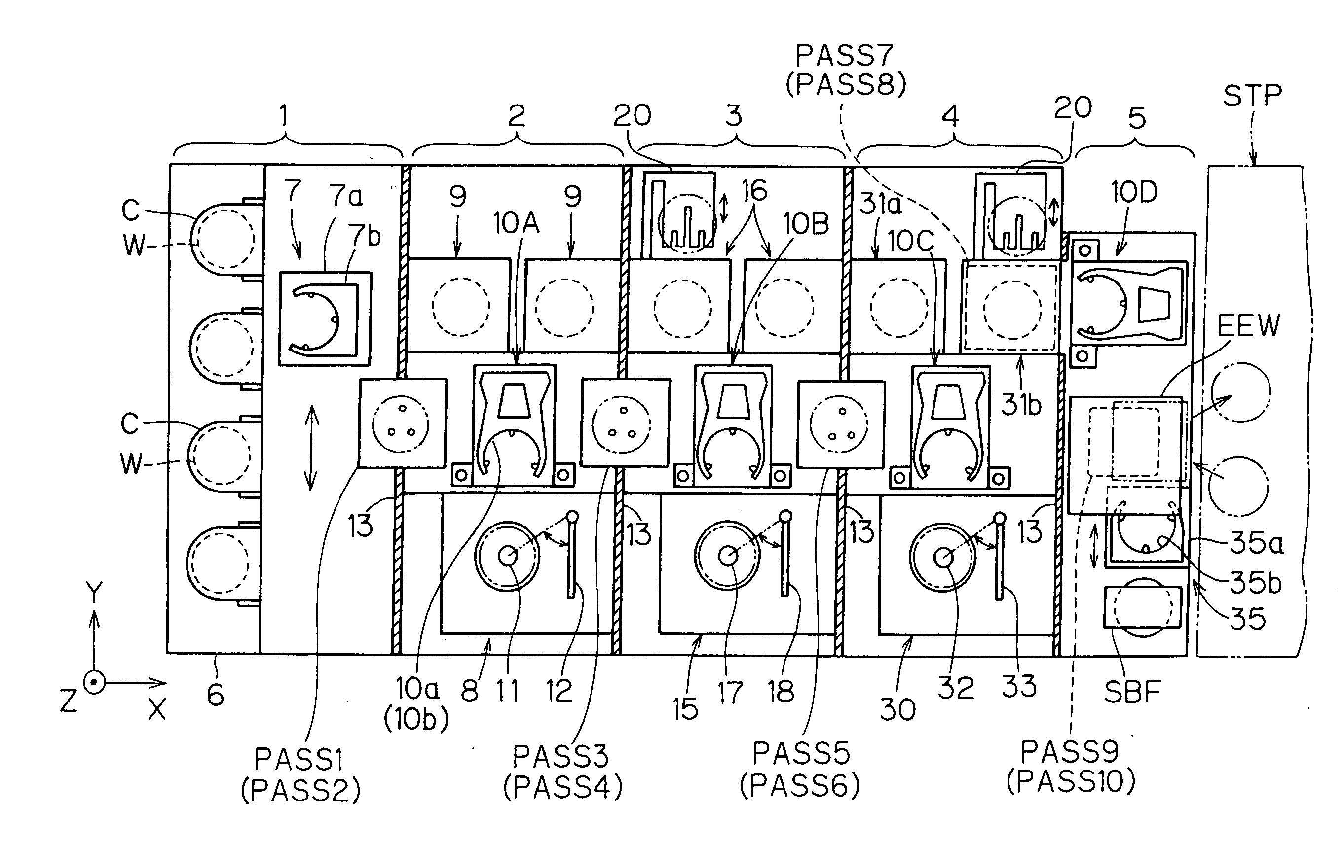
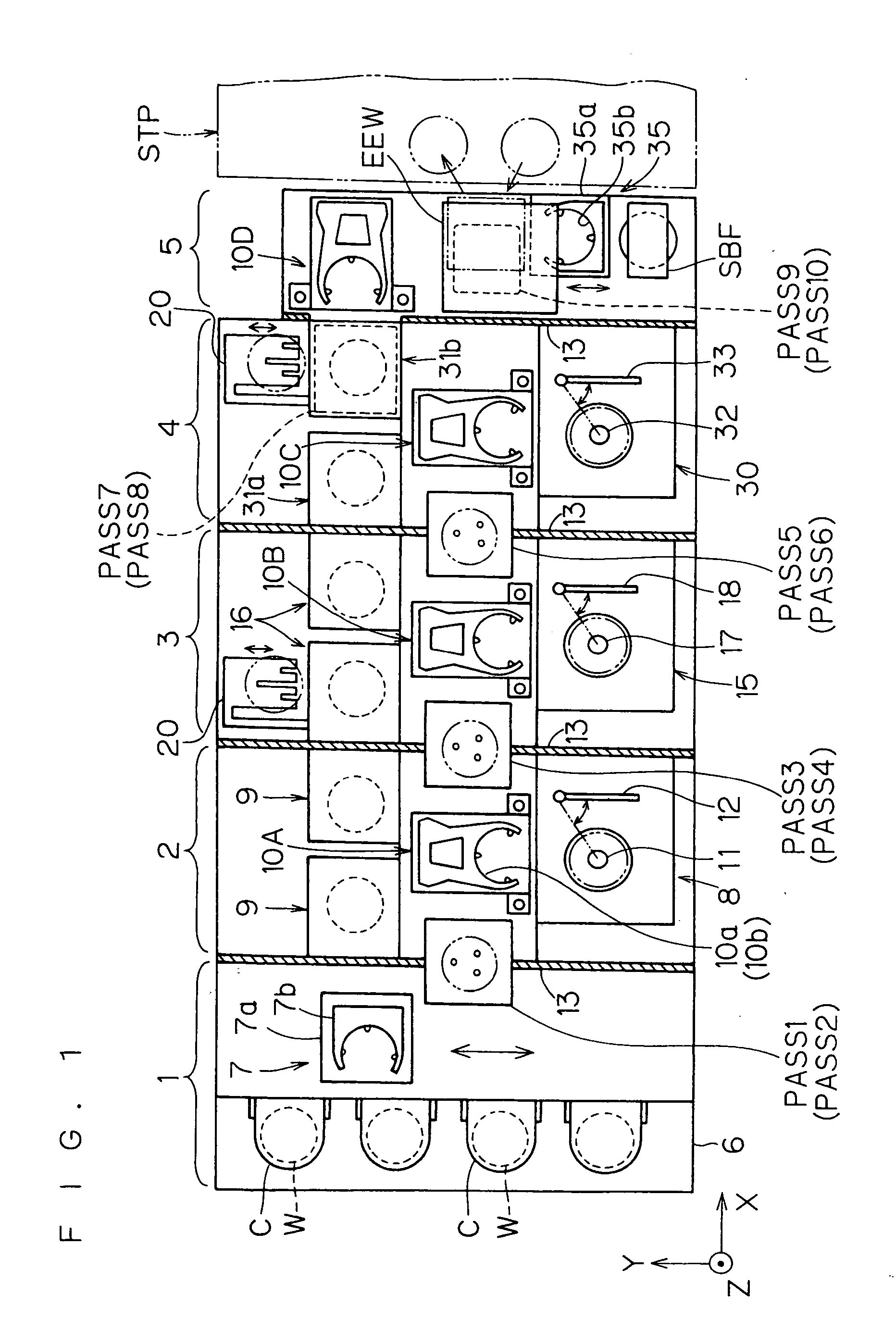
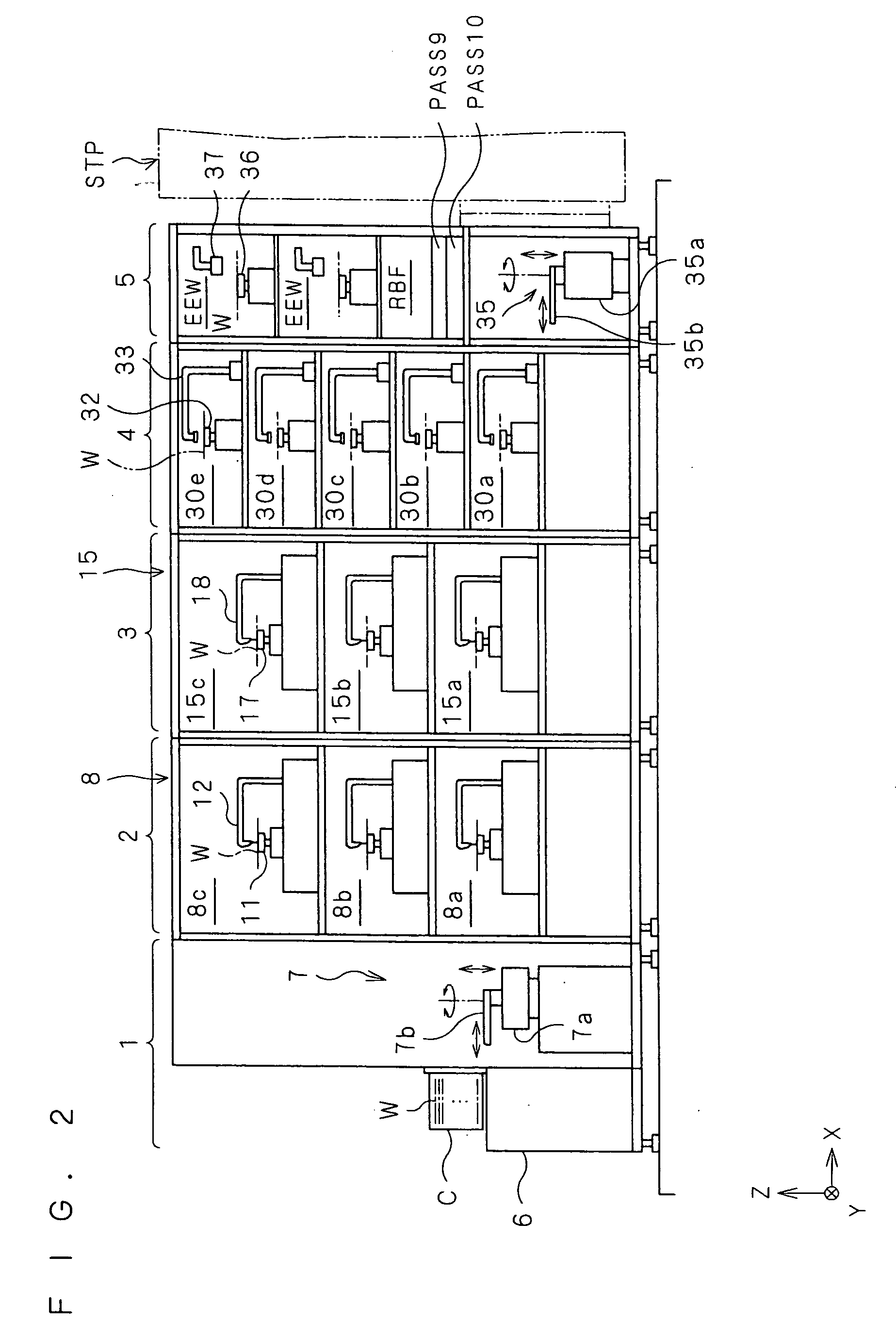
[0045]FIG. 1 is a top plan view of a substrate processing apparatus according to the preferred embodiment of the present invention. FIG. 2 is a front view of a chemical processor in the substrate processing apparatus. FIG. 3 is a front view of a thermal processor in the substrate processing apparatus. FIG. 4 shows a construction around substrate rest parts in the substrate processing apparatus. An XYZ rectangular coordinate system which defines the direction of the Z axis as the vertical direction is additionally shown in FIGS. 1 to 4.
[0046] The substrate processing apparatus according to the preferred embodiment is an apparatus for forming an anti-reflection film and a photoresist film on substrates such as semiconductor wafers by coating and for performing a development process on substrates subjected to a pattern exposure process. The substrates to be ...
PUM
| Property | Measurement | Unit |
|---|---|---|
| Time | aaaaa | aaaaa |
Abstract
Description
Claims
Application Information


