Light emission diode (LED)

a technology of light-emitting diodes and leds, which is applied in the direction of semiconductor devices, lighting and heating apparatus, and semiconductor devices for light sources. it can solve the problems of affecting the junction temperature of light-emitting chips is higher, and the number of distributions of light-emitting chips by unit area is comparatively less to be applicable in ordinary illumination that requires higher luminance. it reduces the junction temperature, improves the service life of leds

Inactive Publication Date: 2005-03-24
FUJIAN JOINLUCK ELECTRONICS ENTERPRISE
View PDF0 Cites 19 Cited by
  • Summary
  • Abstract
  • Description
  • Claims
  • Application Information

AI Technical Summary

Benefits of technology

[0014] Whereas the heat conduction substrate is provided, those light emitting chips are capable of fast dissipating the heat through the heat conduction substrate to lower their junction temperature, thus to increase efficacy and service life of the light emitting chip, and to realize the lay up of more light emitting chips on the unit area. The recess or the trough provided on the heat conduction substrate help converge the light and various circuitries can be arranged among the light emitting chips and / or between light emitting chips and the circuitry depending on the individual application. Furthermore, the light emitting chip can be made into various types of modules for mass production by lot and mounted on the support board depending on the individual application to form a lighting source or light emitting source.

Problems solved by technology

Whereas power dissipation of the LED of the prior art takes place at the frame, power dissipation in the form of heat is poor to cause higher junction temperature of the light-emitting chip and negatively affect the light emitting efficacy and service light of the LED.
Furthermore, the number of the distribution of the light emitting chips by unit area is comparatively lesser to be applicable in the ordinary illumination that requires higher luminance.

Method used


Image

  • Light emission diode (LED)
  • Light emission diode (LED)
  • Light emission diode (LED)

Examples


Embodiment Construction

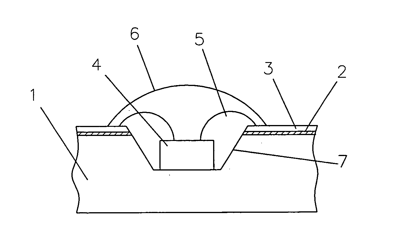
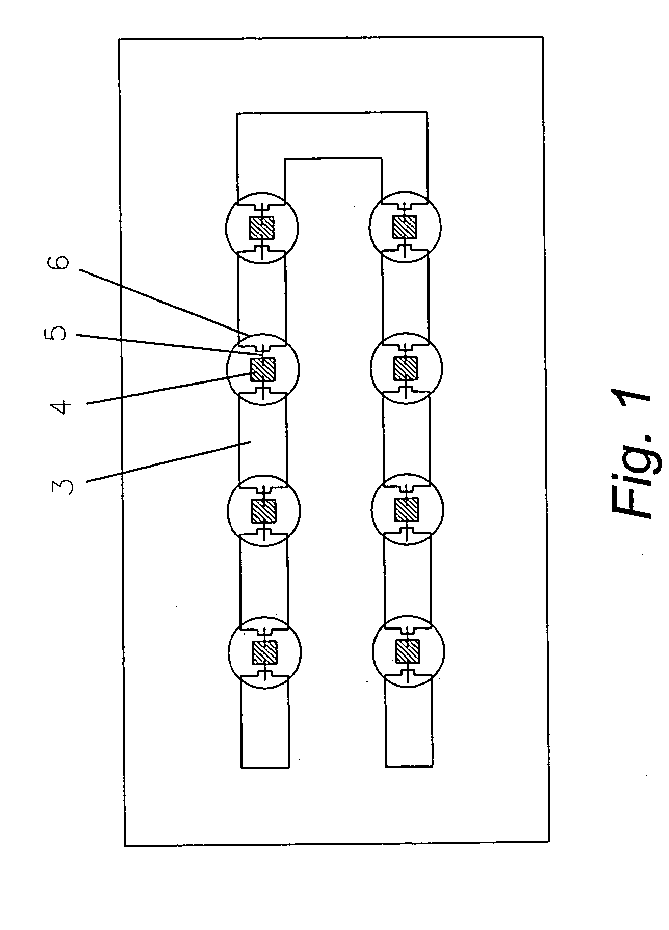
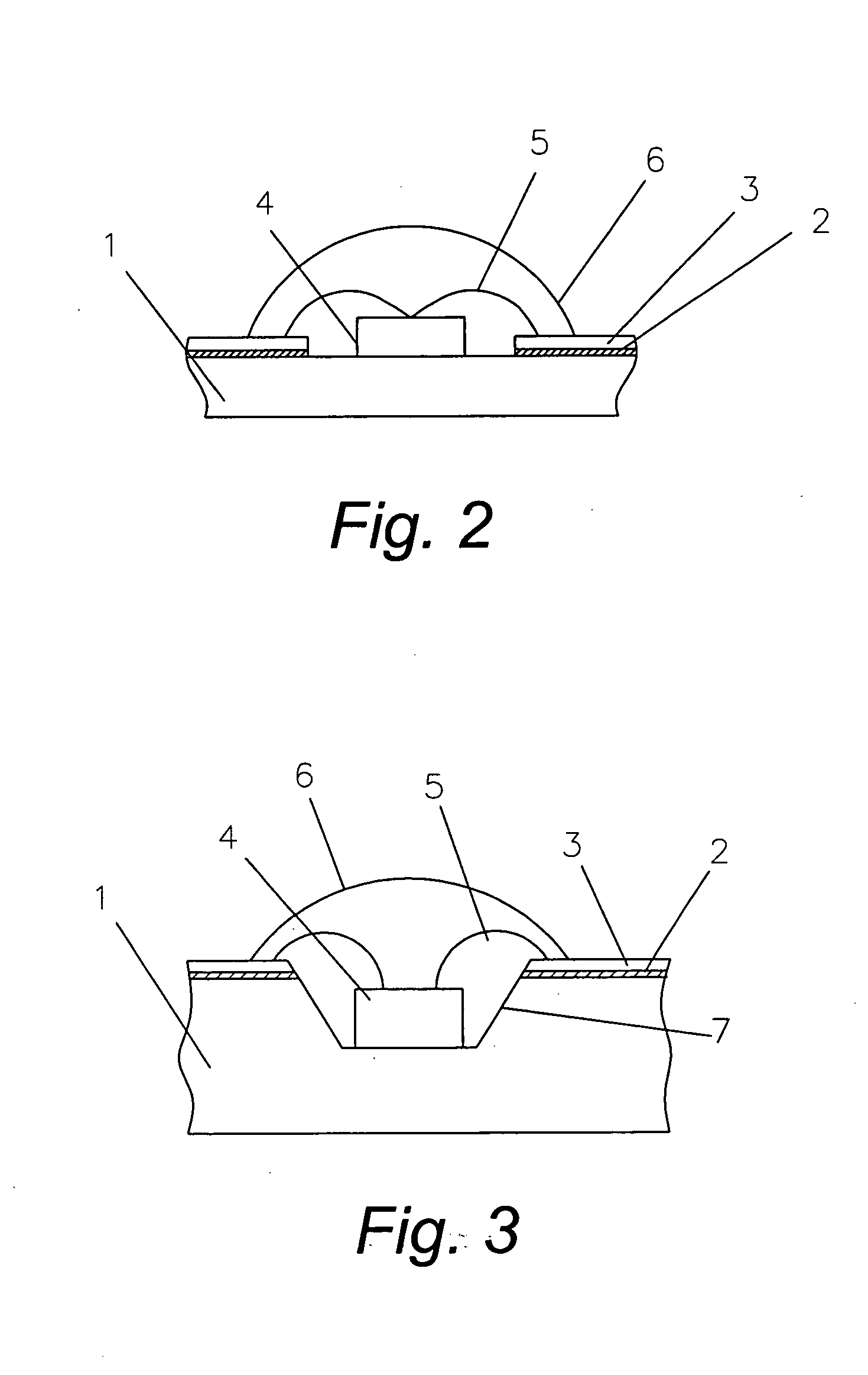
[0027] Referring to FIGS. 1 and 2, a LED of the present invention includes a heat conduction substrate 1; a circuitry 3 is provided on the heat conduction substrate 1; an insulation layer 2 is provided between the heat conduction substrate 1 and the circuitry 3; multiple light emitting chips 4 are arranged among the circuit in the space over the heat conduction substrate; those light emitting chips 4 are each connected to the circuitry 3 by means of a metal conductor 5; and those light emitting chips 4 are covered up with a light permeable protection layer 6.

[0028] The heat conduction substrate 1 is made of ceramic material provided with good aluminum and copper heat conduction property or any other material with good heat conduction property. The insulation layer 2 yields powerful insulation property, and the circuitry 3 on the top of the insulation layer 2 may be related to a copper foil to be etched with various circuits as required.

[0029] Those light emitting chips 4 are arran...


PUM


Abstract

A light emitting diode (LCD) comprised of a heat conduction substrate, a circuitry on the substrate, an insulation layer between the substrate and the circuit, multiple light emitting chips distributed in the space between the circuitry and the substrate, light emitting chips being connected to the circuitry through metallic conductor, and a light permeable protection layer being topped on those light emitting chips to significantly improve its power dissipation effect, lower light emission chip junction temperature, increase light emission efficacy and service life, increase the quantity of the light emission chip of unit area, and improve the light emission efficiency of unit area.

Description

BACKGROUND OF THE INVENTION [0001] (a) Field of the Invention [0002] The present invention is related to a light emitting diode (LCD). [0003] (b) Description of the Prior Art [0004] LED packaging technology of the prior art involves gluing light emission chips to a frame, connection of metallic conductor between chips and frame, packaged with epoxy, and finally having the LEC welded to a PCB using the plug-in package method. Whereas power dissipation of the LED of the prior art takes place at the frame, power dissipation in the form of heat is poor to cause higher junction temperature of the light-emitting chip and negatively affect the light emitting efficacy and service light of the LED. Furthermore, the number of the distribution of the light emitting chips by unit area is comparatively lesser to be applicable in the ordinary illumination that requires higher luminance. Therefore, the LED manufacturing industry has been desperately solving the problem of how to increase LED effic...

Claims


Application Information

Patent Timeline
Patent Type & Authority Applications(United States)
IPC IPC(8): F21K99/00H01L23/28H01L25/075H01L27/15H01L33/00
CPCF21K9/00H01L25/0753H01L2224/48091F21V29/76H01L2924/12041F21V29/2212F21V29/677H01L2924/00014
Inventor HUANG, DE-SEN
Owner FUJIAN JOINLUCK ELECTRONICS ENTERPRISE
Why Eureka
Try Eureka