Plasma display panel and plasma display apparatus
a plasma display and plasma technology, applied in static indicating devices, instruments, gas-filled discharge tubes, etc., can solve the problems of reducing neighboring electrodes may short-circuit, and the current manufacturing technology is not easy to form a constant distance stably, so as to reduce the production yield of the panel
- Summary
- Abstract
- Description
- Claims
- Application Information
AI Technical Summary
Benefits of technology
Problems solved by technology
Method used
Image
Examples
first embodiment
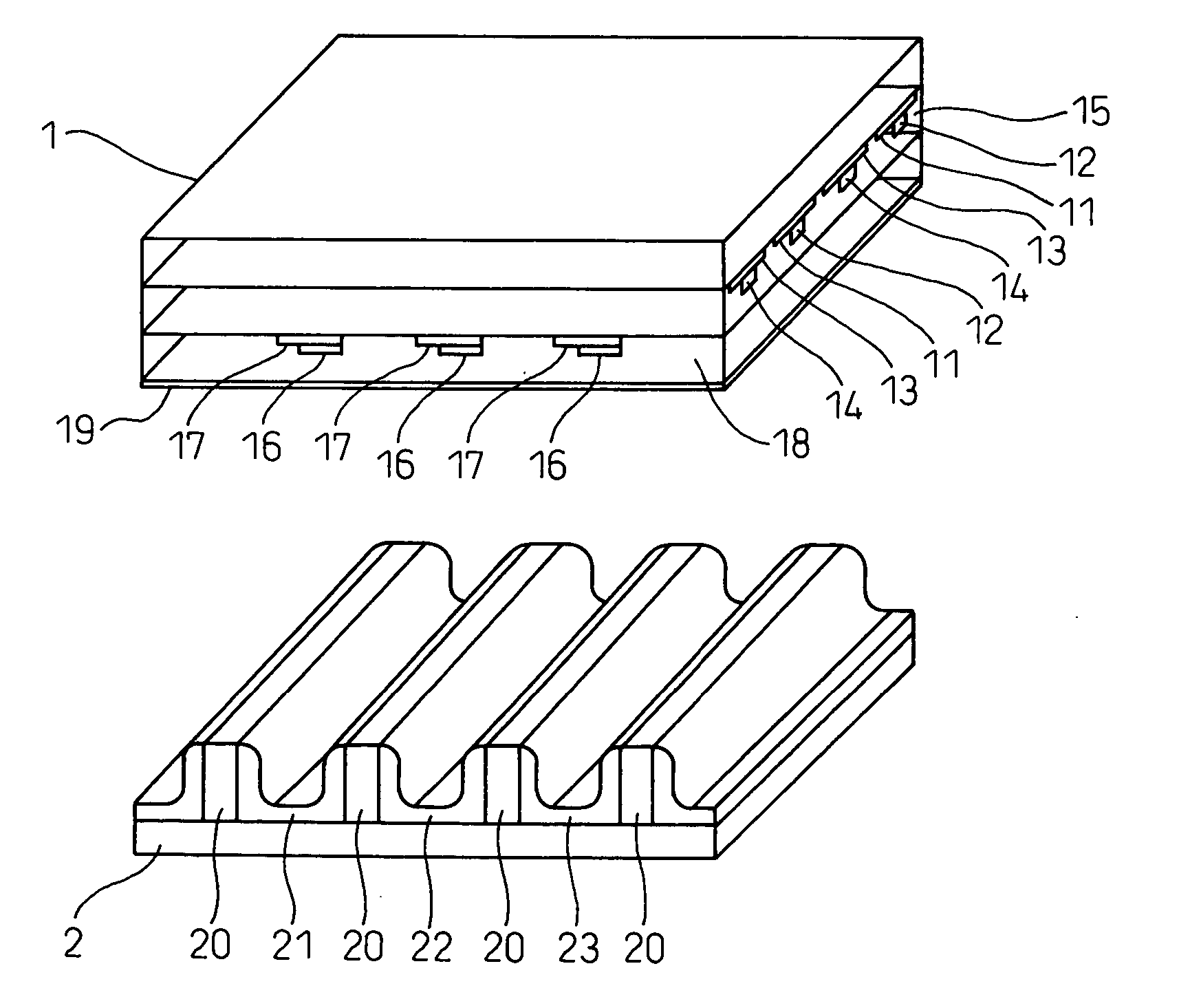
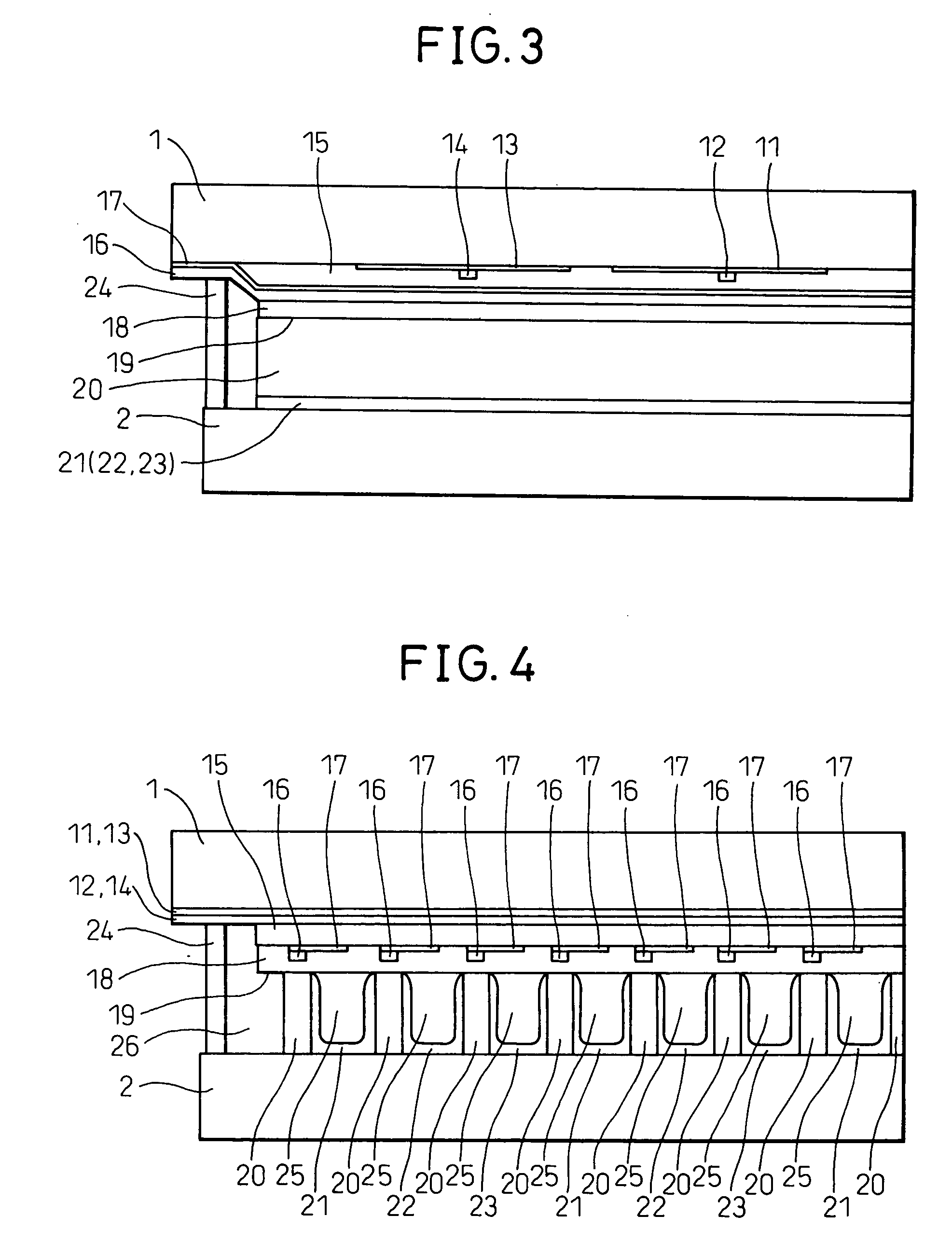
[0091] In the present invention, the present invention is applied to an ALIS system PDP device described in Japanese Patent No. 2801893, in which third electrodes (address electrodes) are provided on a first substrate (a transparent substrate) together with first and second electrodes (X and Y electrodes). As the ALIS system is described in the above-mentioned document, a detailed explanation is not given here.
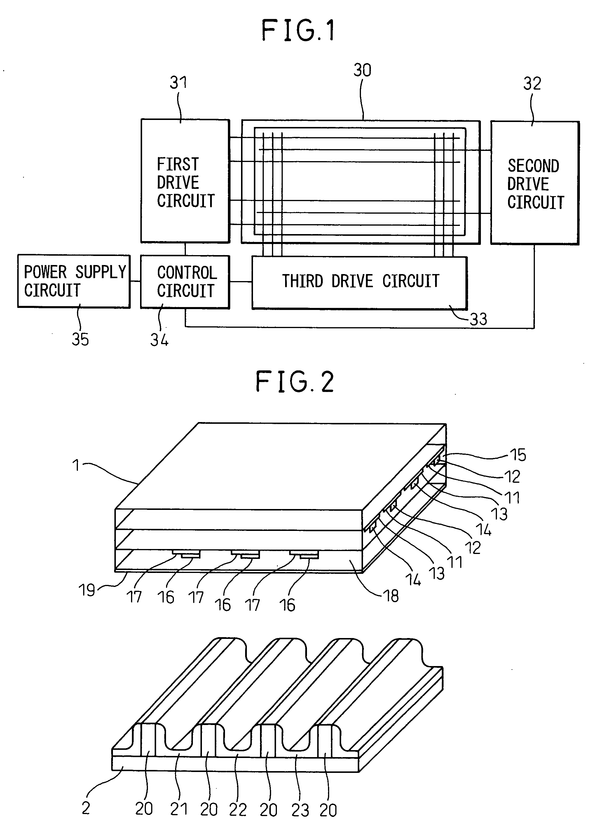
[0092]FIG. 1 is a diagram showing a general configuration of a plasma display apparatus (PDP apparatus) in the first embodiment of the present invention. As shown schematically, a plasma display panel 30 comprises a group of first electrodes (X electrodes) and a group of second electrodes (Y electrodes) extending in the transverse direction (the direction of the length) and a group of third electrodes (address electrodes) extending in the longitudinal direction. The group of X electrodes and the group of Y electrodes are arranged by turns and the number of the X electrodes is ...
third embodiment
[0140] In the third embodiment, since the distance between the facing edges of the Y discharge electrode 11 and the X discharge electrode 13 is constant and it is comparatively large, no short-circuit occurs even if the positions and sizes of the Y and X discharge electrodes vary due to the production errors. Therefore, a production yield does not decrease.
[0141] Further, since the facing edges of the Y discharge electrode 11 and the address discharge electrode 17 are formed to gradually change a distance, a position at which the Paschen minimum condition is satisfied always exists. Therefore, the address discharge start voltage can be reduced in a same way as the first embodiment.
[0142] Further, the distance d between the facing edges of the Y discharge electrode 11 and the address discharge electrode 17 is narrower at a side nearer to the X discharge electrode 13. As described in the first embodiment, according to this shapes of the electrodes, the discharge between the Y dischar...
fifth embodiment
[0157]FIG. 20 is an exploded perspective view of a plasma display panel (PDP) according to the As shown schematically, on the front (first) glass substrate 1, the first (X) bus electrodes 14 and the second (Y) bus electrodes 12 extending in the transverse direction are arranged by turns in parallel to each other and the X and Y discharge electrodes 13 and 11 are provided so as to overlap the bus electrodes. On the discharge electrodes 13 and 11 and the bus electrodes 14 and 12, the first dielectric layer 15 is provided so as to cover these electrodes. The first dielectric layer 15 is composed of SiO2 etc., formed by the vapor phase film deposition method. The thickness of the first dielectric layer is approximately less than or equal to 10 μm. The protective layer 19 such as MgO is further formed thereon.
[0158] On the back substrate 2, on the other hand, the third (address) electrodes 36, which are metal layers, are provided so as to perpendicularly intersect the X and Y bus electr...
PUM
 Abstract
Description
Claims
Application Information


