Method for manufacturing electronic device and method for manufacturing glass laminate

A technology of electronic devices and manufacturing methods, applied in semiconductor/solid device manufacturing, chemical instruments and methods, glass/slag layered products, etc., can solve problems such as short circuit rise, circuit electrode disconnection, and difficulty in ensuring reliability, etc., to achieve Excellent flatness and the effect of suppressing the decrease in production yield

Active Publication Date: 2016-09-28
ASAHI GLASS CO LTD
View PDF6 Cites 0 Cited by
  • Summary
  • Abstract
  • Description
  • Claims
  • Application Information

AI Technical Summary

Problems solved by technology

[0006] On the other hand, as described in paragraph 84 of Patent Document 2, when there is waviness larger than 0.100 μm on the surface of the glass, it is difficult to accurately pattern the circuit electrodes and the like formed on the surface, and as a result, the circuit The probability of electrode disconnection and short circuit increases, the yield of electronic devices such as liquid crystal displays decreases, and it is difficult to guarantee their reliability

Method used


Image

  • Method for manufacturing electronic device and method for manufacturing glass laminate
  • Method for manufacturing electronic device and method for manufacturing glass laminate
  • Method for manufacturing electronic device and method for manufacturing glass laminate

Examples


Embodiment 1

[0198] Prepare a glass substrate ("AN100", linear expansion coefficient 38×10 -7 A non-alkali glass plate at / °C: manufactured by Asahi Glass Co., Ltd.) was used as a support substrate, and the surface was cleaned with purified water and UV to obtain a surface-cleaned support substrate.

[0199] Next, straight-chain vinylmethyl polysiloxane ("VDT-127", viscosity at 25°C: 700-800 cP (centipoise): manufactured by AZMAX Corporation, 1 mol of organopolysiloxane as component (A) The mol% of the vinyl group: 0.325), and the linear methylhydrogen polysiloxane "HMS-301" as the component (B), the viscosity at 25°C of 25-35cP (centipoise): manufactured by AZMAX Corporation , the number of hydrogen atoms bonded to silicon atoms in 1 molecule: 8), mixed in such a way that the molar ratio of all vinyl groups to hydrogen atoms bonded to all silicon atoms (hydrogen atoms / vinyl groups) is 0.9, With respect to 100 parts by weight of this siloxane mixture, 1 part by weight of a silicon compoun...

Embodiment 2

[0208] With respect to 100 parts by weight of the mixed solution of the organopolysiloxane composition obtained in the same steps as in Example 1, 43 parts by weight of heptane was added to prepare a mixed solution, and the obtained mixed solution was used with a die coater (coating speed: 40mm / s, GAP140μm, coating pressure 50kPa) onto the support substrate, let it stand at room temperature for 10 minutes, and then heat it at 180°C in the atmosphere for 60 minutes to cure to form a 15μm cured silicone resin layer. Other than that, in the same procedure as in Example 1, a glass laminate was produced and polished, and the polished glass substrate was separated. The various results are summarized in Table 1. Wherein, the filter centerline waviness (W CA ) is at the same level as the filter centerline waviness of the resin layer and is 0.100 μm or less.

Embodiment 3

[0210] After coating the mixed solution on the support substrate with a die coater, let it stand at room temperature for 30 minutes, and then heat it at 180° C. in the air for 60 minutes to cure it to form a 15 μm cured silicone resin layer. In addition, In the same procedure as in Example 2, a glass laminate was prepared and polished, and the polished glass substrate was separated. The various results are summarized in Table 1. Wherein, the filter centerline waviness (W CA ) is at the same level as the filter centerline waviness of the resin layer and is 0.100 μm or less.


PUM

PropertyMeasurementUnit
thicknessaaaaaaaaaa
thicknessaaaaaaaaaa
viscosityaaaaaaaaaa

Abstract

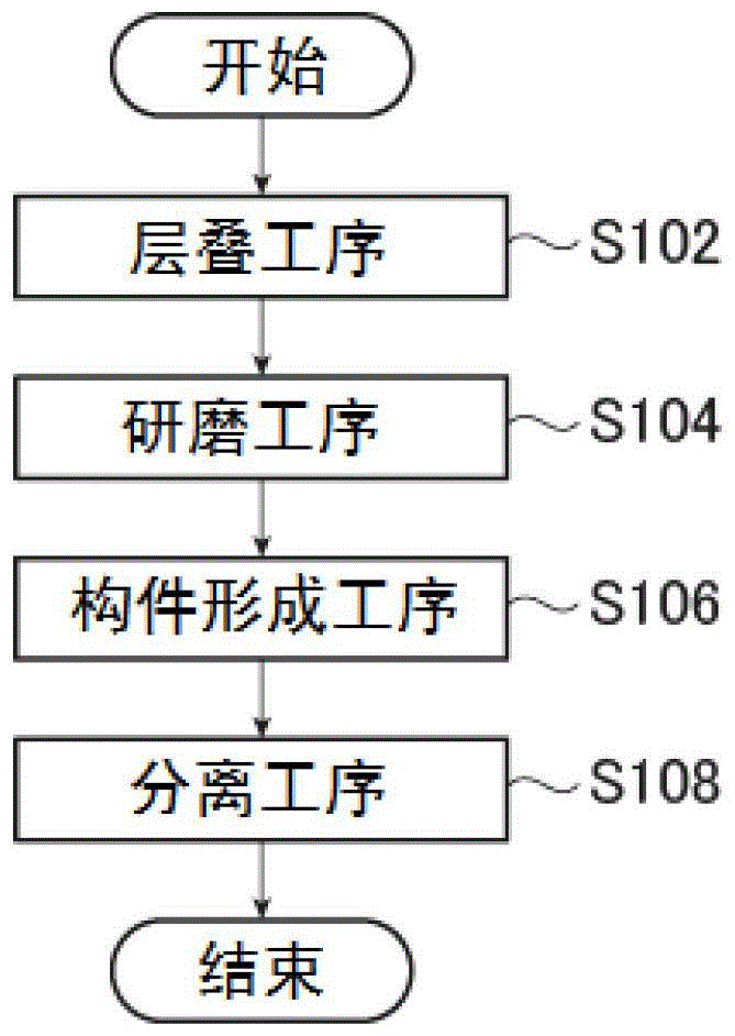
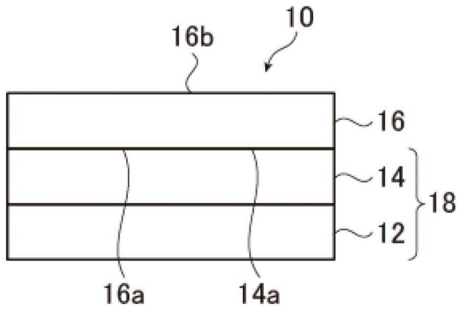
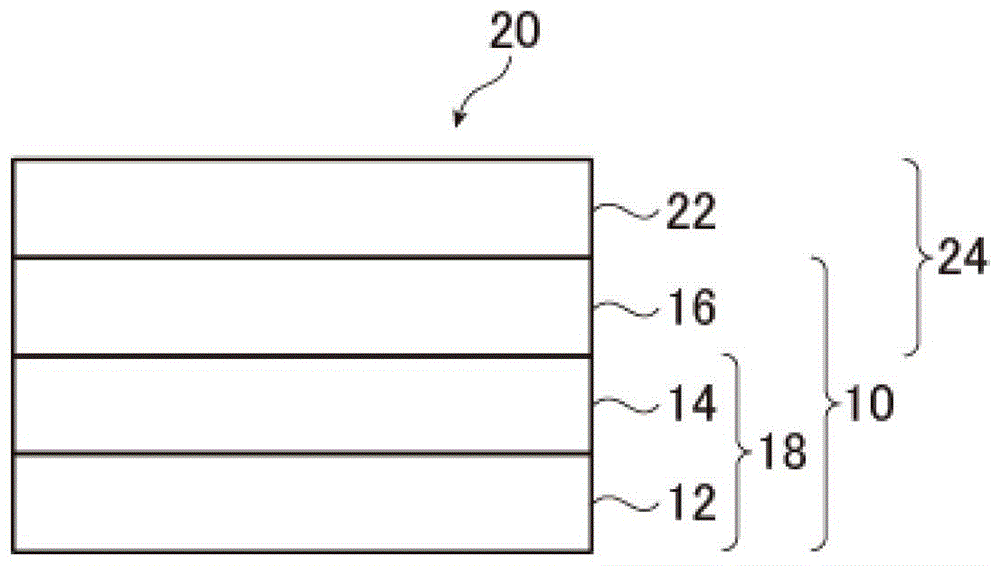
PROBLEM TO BE SOLVED: To provide a method for manufacturing a glass substrate having an electronic device component included therein which, when an electronic device component is formed and even after a glass substrate having the electronic device component formed thereon is separated, excels in the flatness of a glass substrate surface and can therefore restrain a decline in the production yield of the electronic device component.SOLUTION: An electronic device manufacturing method comprises: a lamination step of laminating a resin layer included support substrate 18 and a glass substrate 16 closely one on top of another to obtain a glass laminate 10; a polishing step of polishing a second principal plane of the glass substrate; a component formation step of forming an electronic device component 22 on the polished second principal plane; and a separation step of separating the glass substrate 16 having the electronic device component 22 laminated thereon and the resin layer included support substrate 18 from each other to obtain an electronic device 24 including the glass substrate 16 and the electronic device component 22. In the electronic device manufacturing method, surface waviness on an exposed surface of a resin layer 14 is 0.1 μm or less in wave filtration center line waviness (W).

Description

technical field [0001] The present invention relates to a method of manufacturing an electronic device and a method of manufacturing a glass laminate. Background technique [0002] In recent years, devices (electronic devices) such as solar cells (PV), liquid crystal panels (LCD), and organic EL panels (OLED) have been reduced in thickness and weight, and glass substrates used in these devices have also been reduced in thickness. If the strength of the glass substrate is insufficient due to thinning, the handling properties of the glass substrate will decrease in the manufacturing process of the device. [0003] Therefore, conventionally, a method of thinning the glass substrate by chemical etching after forming device members (such as thin film transistors) on a glass substrate thicker than the final thickness has been widely used. However, in this method, for example, when the thickness of one glass substrate is reduced from 0.7 mm to 0.2 mm and then reduced to 0.1 mm, mo...

Claims


Application Information

Patent Timeline
Patent Type & Authority Patents(China)
IPC IPC(8): B32B37/02B32B17/10B32B17/06G02F1/13H01L21/77C03C3/085C03C3/087C03C3/091
CPCY02E10/50B24B37/04B32B7/06B32B17/10018B32B17/10798C03C3/093G02F1/1333G02F1/133302
Inventor 内田大辅
Owner ASAHI GLASS CO LTD
Why Eureka
Try Eureka