Coupled-inductance differential amplifier

a technology of differential amplifier and coupled inductance, which is applied in the direction of amplifiers, amplifiers with semiconductor devices/discharge tubes, electric devices, etc., can solve the problems of affecting the frequency response of differential amplifiers. the effect of common mode rejection

Active Publication Date: 2005-03-24
AVAGO TECH INT SALES PTE LTD
View PDF9 Cites 118 Cited by
  • Summary
  • Abstract
  • Description
  • Claims
  • Application Information

AI Technical Summary

Problems solved by technology

Unfortunately, the physical space taken up by the winding structures of individual inductor components may hinder attempts to decrease the physical size of a differential amplifier.
The size limitations imposed by the physical dimensions of inductor components may be a particular hindrance in the design of differential amplifiers contained on integrated circuit chips.
In addition, electrical interactions that may occur between individual inductor components may alter the frequency response of a differential amplifier away from its desired response.

Method used


Image

  • Coupled-inductance differential amplifier
  • Coupled-inductance differential amplifier
  • Coupled-inductance differential amplifier

Examples


Embodiment Construction

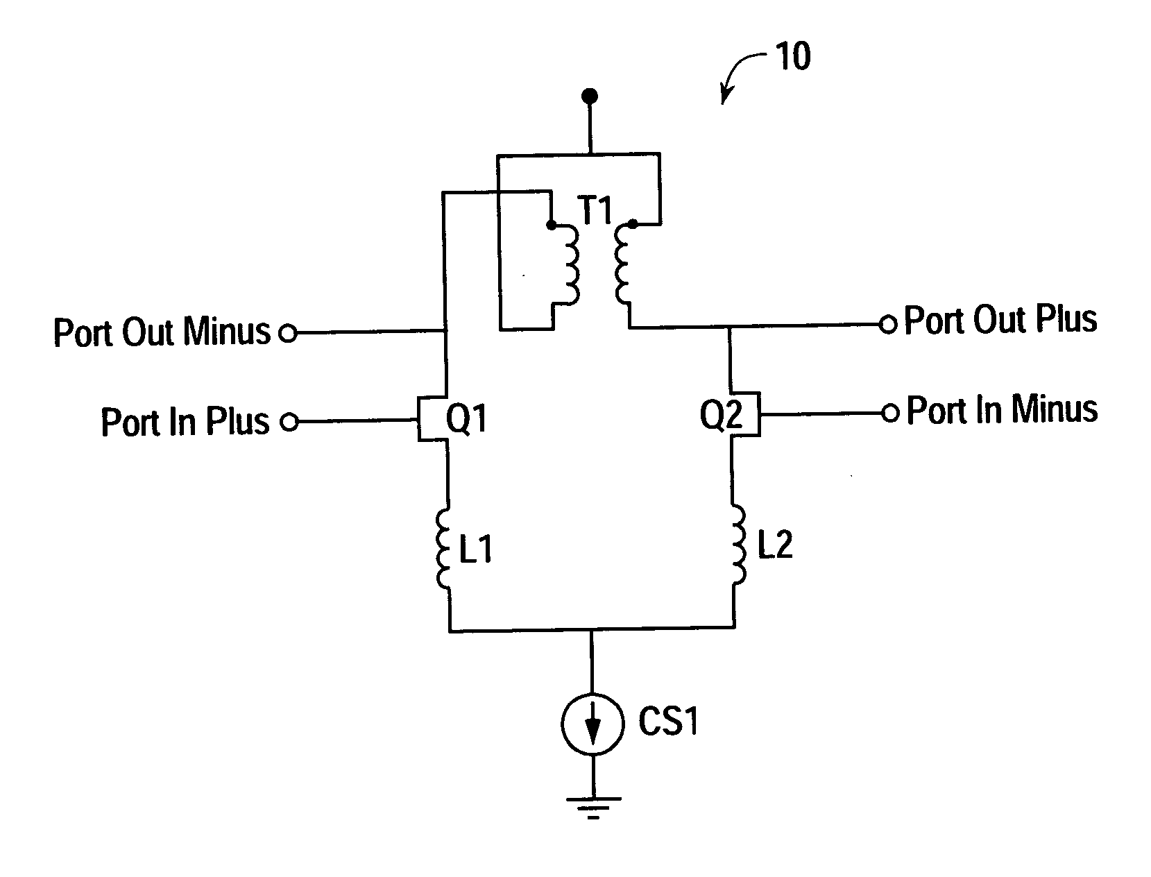
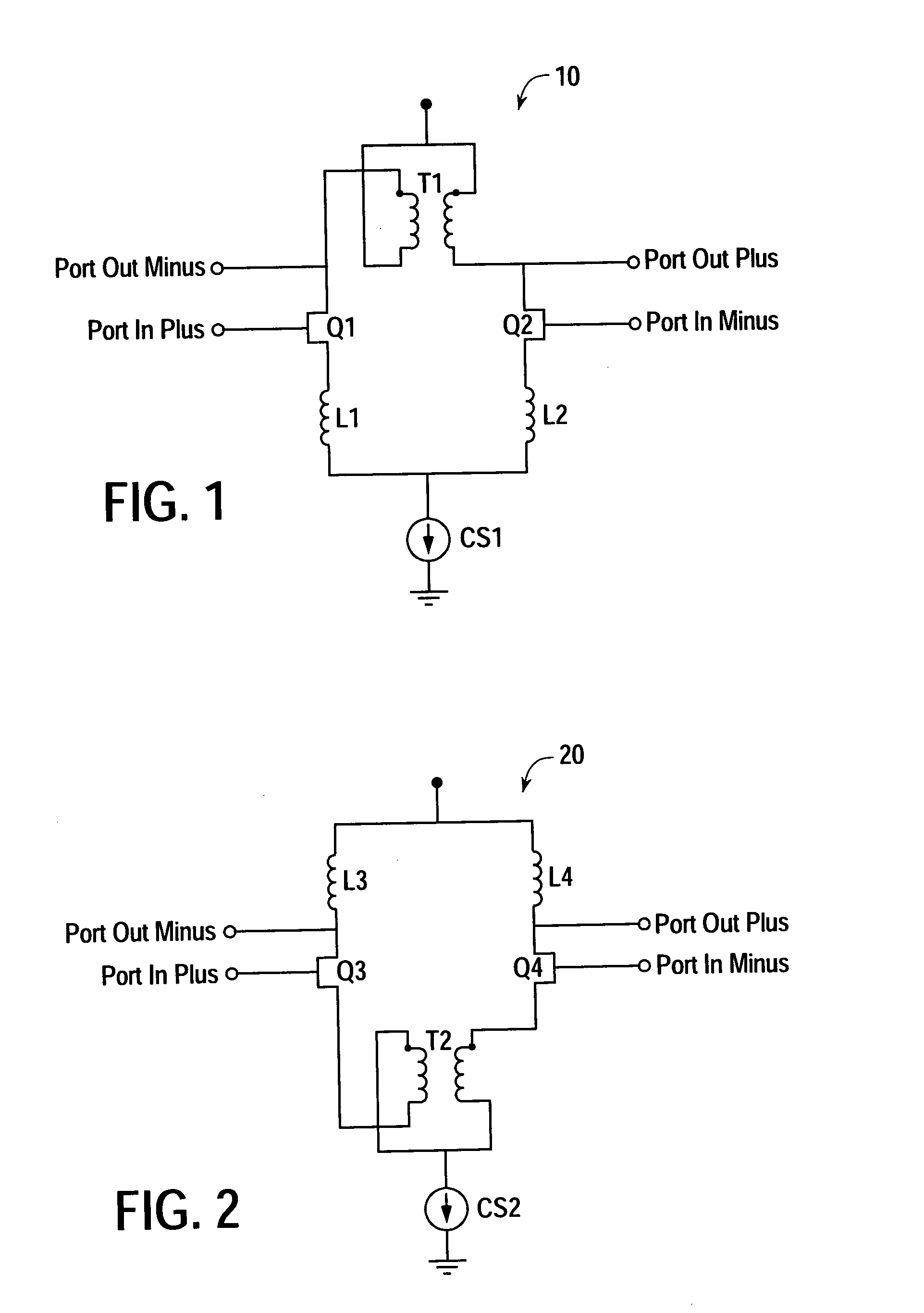
[0010]FIG. 1 shows a differential amplifier 10 according to the present teachings. The differential amplifier 10 includes a pair of transistors Q1 and Q2. The transistors Q1 and Q2 may be field-effect transistors (FETs) or alternatively bipolar junction transistors (BJTs). The differential amplifier 10 generates a differential output signal at its output ports (PORT OUT PLUS and PORT OUT MINUS) in response to a differential input signal received at its input ports (PORT IN PLUS and PORT IN MINUS).

[0011] The differential amplifier 10 includes a pair of mutually coupled inductors in the form of a transformer T1. The mutually coupled inductors in the transformer T1 in the embodiment shown are used for biasing the transistors Q1 and Q2 and for providing impedance matching at the output ports PORT OUT PLUS and PORT OUT MINUS of the differential amplifier 10.

[0012] The transformer T1 is wired so that the effective inductances of its individual inductor windings are augmented by mutual c...


PUM


Abstract

A differential amplifier that employs mutually coupled inductors to provide desired levels of inductance in a substantially smaller form factor in comparison to individual inductor components. Mutually coupled inductors according to the present teachings may also be used to increase common mode rejection in a differential amplifier.

Description

BACKGROUND [0001] Differential amplifiers may be employed in a variety of electronic circuits including circuits that operate at radio frequency (RF), microwave, and millimeter wave frequencies. A differential amplifier may include a pair of transistors that generate a differential output signal at a pair of output ports in response to a differential input signal received at a pair of input ports. [0002] A prior differential amplifier may include a set of individual inductor components. For example, inductor components may be used for transistor biasing in a differential amplifier. In addition, inductor components may be used for impedance matching at the input and / or output ports of a differential amplifier. Inductor components may also be used for noise reduction in a differential amplifier. [0003] Unfortunately, the physical space taken up by the winding structures of individual inductor components may hinder attempts to decrease the physical size of a differential amplifier. The...

Claims


Application Information

Patent Timeline
Patent Type & Authority Applications(United States)
IPC IPC(8): H03F1/26H03F3/195H03F3/45
CPCH03F3/45381H03F2203/45731H03F2203/45662
Inventor VICE, MICHAEL W.
Owner AVAGO TECH INT SALES PTE LTD
Why Eureka
Try Eureka