Display device and driving circuit for the same display method

a display device and driving circuit technology, applied in the field of matrix display devices and methods, can solve the problems of insufficient writing period and may not be guaranteed, and achieve the effects of reducing the level shift of the parasitic capacitor, avoiding a rapid fall of scanning signals, and high-quality displays

Active Publication Date: 2005-03-24
UNIFIED INNOVATIVE TECH
View PDF4 Cites 28 Cited by
  • Summary
  • Abstract
  • Description
  • Claims
  • Application Information

AI Technical Summary

Benefits of technology

[0052] Accordingly, as with the foregoing display device and / or display method of at least one embodiment, the scanning signal has a falling waveform partly varying with a slope, thereby avoiding a rapid fall of the scanning signal. On this account, the level shift of the pixel electrode caused by the parasitic capacitor is reduced, thereby achieving high-definition and high-quality display.
[0053] Further, since the falling waveform of the scanning signal first falls substantially vertically before falling with a slope, it is possible to ensure sufficient voltage (level) for allowing the scanning signal to supply the data signal to a pixel via the switching element such as a thin film transistor. On this account, the writing of the data signal to the pixel electrode may be securely carried out even when the writing period for each scanning signal is reduced. Therefore, this structure may be immune to defect due to reduction of writing period in a display device of higher resolution.

Problems solved by technology

Accordingly, if the writing period for each scanning signal is reduced in order to obtain a higher-resolution, a sufficient writing period may not be ensured.

Method used


Image

  • Display device and driving circuit for the same display method
  • Display device and driving circuit for the same display method
  • Display device and driving circuit for the same display method

Examples


embodiment 1

[0069] The following will explain another embodiment of the present invention with reference to FIG. 2. For ease of explanation, materials having the equivalent functions as those shown in the drawings pertaining to Embodiment 1 above will be given the same reference symbols, and explanation thereof will be omitted here.

REFERENCE EXAMPLE

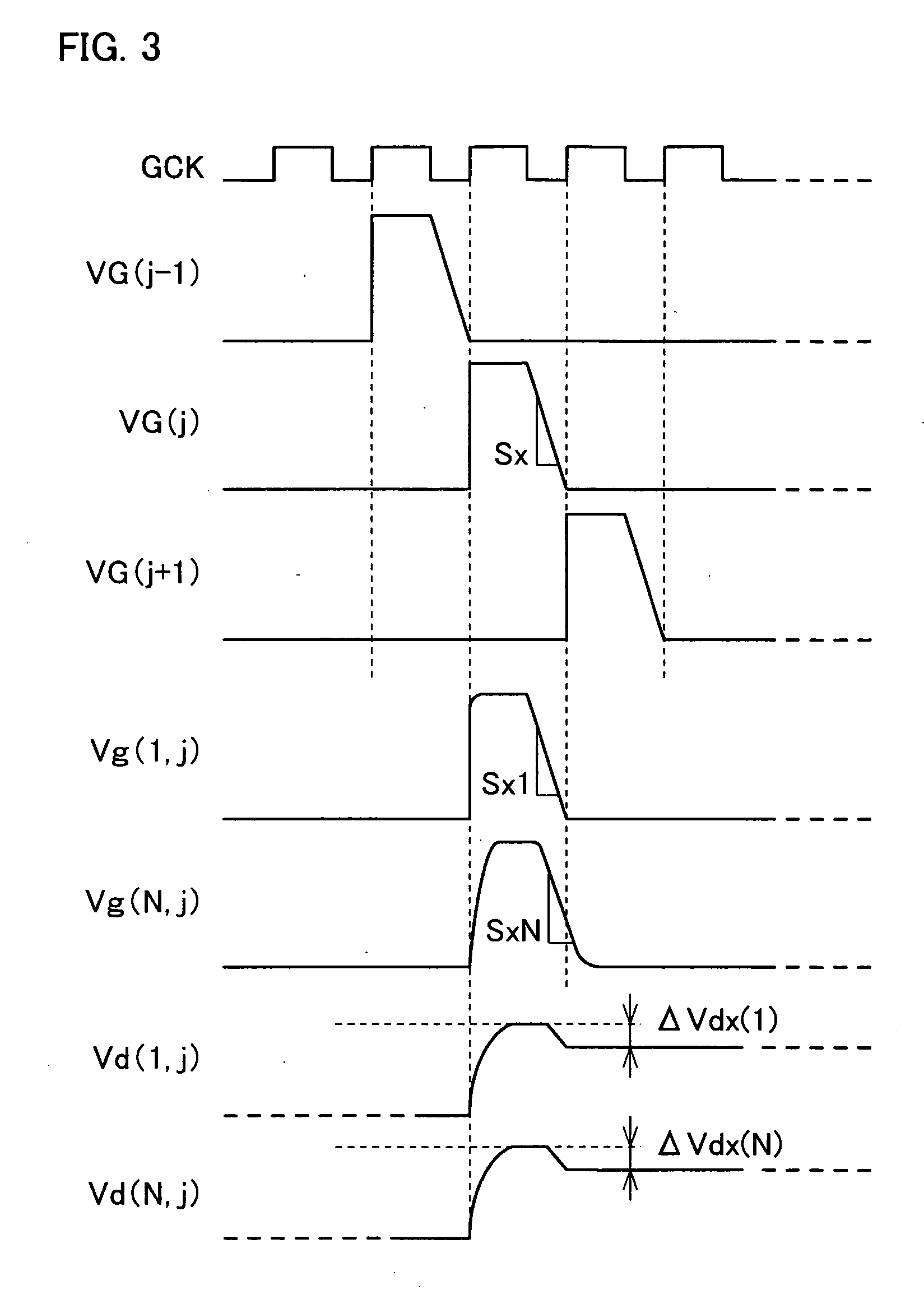
[0070] With reference to FIGS. 3 and 4, the following describes a reference example for the embodiment according to the present invention. In FIG. 3, GCK expresses a clock signal.

[0071]FIGS. 3 and 4 show various waveforms of a scanning signal line driving circuit according to the present reference example. The waveforms include output waveforms VG(j−1), VG(j) and VG(j+1); a scanning waveform Vg(1, j) in the vicinity of the input of the scanning signal line; a scanning signal line waveform Vg(N, j) in the vicinity of the terminating end of the scanning signal line; and the respective pixel potentials Vd(1, j) and Vd(N, j). As shown in FIG. 3, the ou...

embodiment

[0084] [Embodiment]

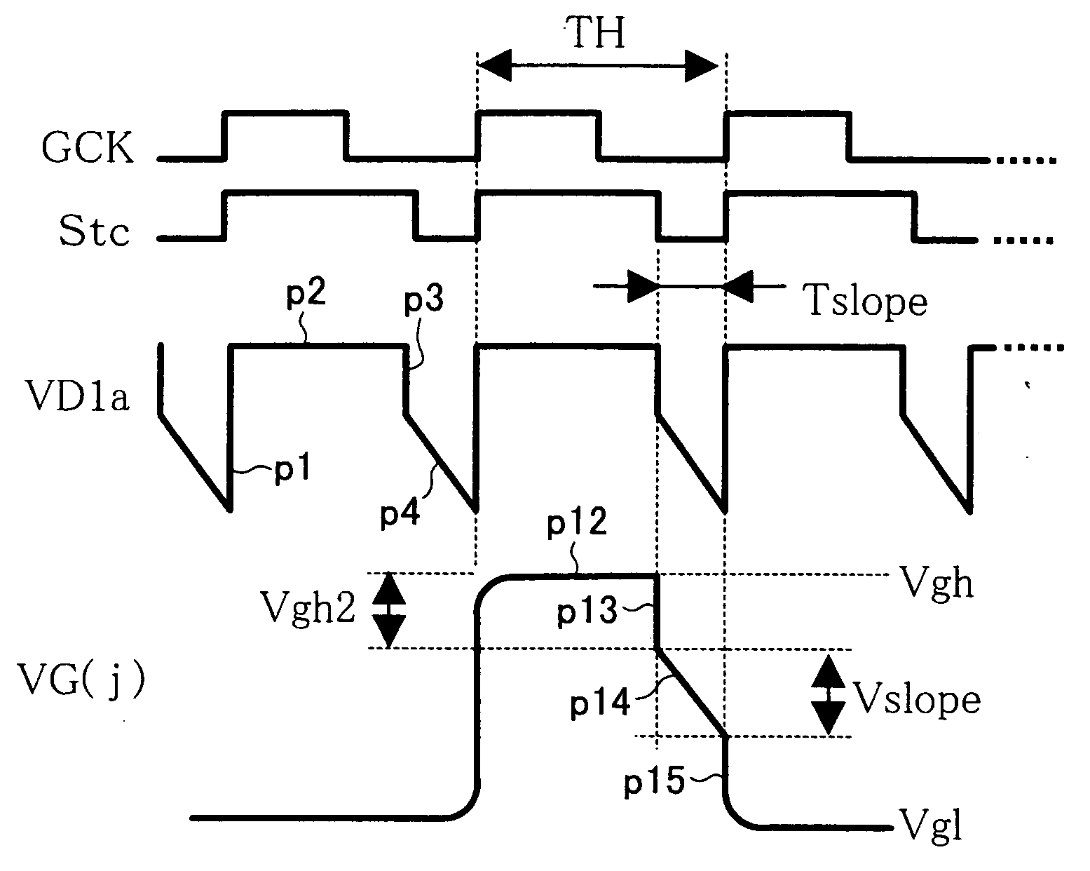
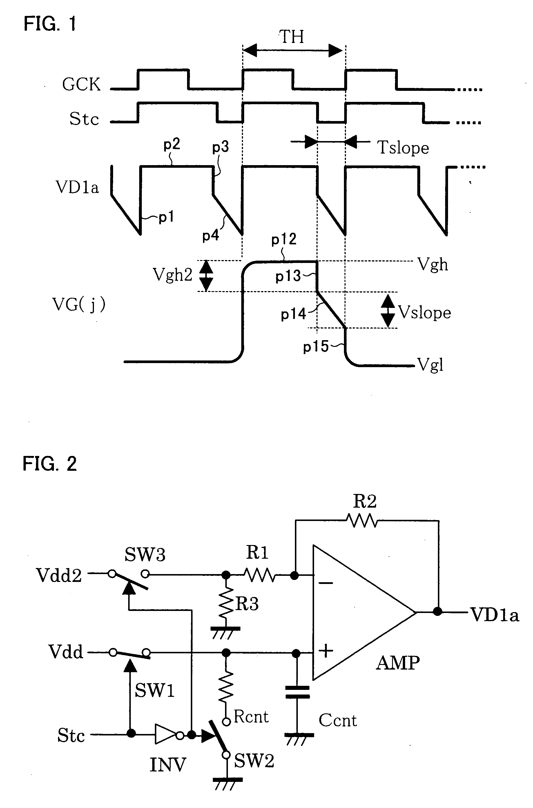
[0085] One embodiment of the present invention is described below mainly with reference to FIGS. 1 and 2, as an example using a conventional general-purpose low-cost scanning signal line driving circuit (gate driver). FIG. 2 is a circuit diagram illustrating a structure of a major part of the scanning signal line driving circuit of the present embodiment, in other words, a signal production circuit included in the scanning signal line driving circuit. FIG. 1 is a waveform diagram of the major part of the scanning signal line driving circuit of the embodiment of the present invention shown in FIG. 2. Note that, according to the circumstances, the explanation below also uses the drawings referred in the explanation of the prior art.

[0086] As explained above with reference to FIG. 6, a conventional scanning signal line driving circuit (gate driver) is arranged such that the gate-ON-voltage Vgh and the gate-OFF-voltage Vgl are supplied to the input terminals VD1 and ...


PUM

PropertyMeasurementUnit
ON-voltageaaaaaaaaaa
OFF-voltageaaaaaaaaaa
gate-ON-voltageaaaaaaaaaa

Abstract

A display device is for carrying out display by supplying a data signal, that is supplied from a video signal line, to one of a plurality of pixel electrodes via a switching element, and by supplying a scanning signal for controlling ON/OFF state of the switching element to the switching element via a scanning signal line that is orthogonal to the video signal line and is connected to the switching element. When the scanning signal is outputted to the scanning signal line, the scanning signal has a falling waveform that first falls substantially vertically from an ON-level of the switching element in a direction of an OFF-level of the switching element, and then starts falling with a slope, and again falls substantially vertically before reaching the OFF-level of the switching element. As such, the writing of the data signal to the pixel electrode may be securely carried out even when the writing period for each scanning signal is reduced, thereby displaying a high-quality image.

Description

[0001] This Nonprovisional application claims priority under 35 U.S.C. § 119(a) on Patent Application No. 2003 / 325879 filed in Japan on Sep. 18, 2003, the entire contents of which are hereby incorporated by reference. FIELD OF THE INVENTION [0002] The present invention generally relates to a matrix display device and method. Particularly, the present invention relates to a display device having a switching element such as a thin film transistor for each of the display pixels, and also to the driving circuit and the display method thereof. BACKGROUND OF THE INVENTION [0003] A liquid crystal display device is widely used as a display device of a TV, a monitor of a personal computer etc. Particularly, a liquid crystal display device having a switching element such as a thin film transistor (hereinafter also referred to as a TFT) offers superior image display even with a larger number of display pixels, without causing crosstalk between adjacent display pixels. [0004]FIG. 5 shows this t...

Claims


Application Information

Patent Timeline
Patent Type & Authority Applications(United States)
IPC IPC(8): G02F1/1368G02F1/133G09G3/20G09G3/32G09G3/36
CPCG09G3/3208G09G3/3648G09G2320/0223G09G2310/066G09G2320/0219G09G3/3677G09G3/36
Inventor MIZUMAKI, HIDETAKA
Owner UNIFIED INNOVATIVE TECH
Why Eureka
Try Eureka