Unipolar, intraband optoelectronic transducers with micro-cavity resonators

an optoelectronic transducer and micro-cavity technology, applied in the direction of optical resonator shape and construction, semiconductor laser arrangement, semiconductor laser, etc., can solve the problems of large device size, inefficient detector of vertical illumination, and design that does not address the large size of the device, so as to achieve a much wider potential impact

Active Publication Date: 2005-03-24
ALCATEL-LUCENT USA INC +1
View PDF11 Cites 24 Cited by
  • Summary
  • Abstract
  • Description
  • Claims
  • Application Information

AI Technical Summary

Benefits of technology

[0019] Although one immediate advantage of our invention is the realization of surface-emitting ISB lasers, the potential impact is much broader. The dimensions of our resonators are greatly scaled down (e.g., ˜50-100 μm) in comparison with those used in standard ISB technology (e.g., 1-3 mm), opening the way for the miniaturization and on-chip integration of ISB lasers for applications involving the use of multi-wavelength 2D ISB laser arrays for spectroscopy and imaging. For this reason we refer to our resonators as micro-cavity resonators.

Problems solved by technology

Previous attempts to develop surface-emitting QC lasers have made use of second-order Bragg gratings superimposed on conventional edge-emitting QC lasers, but those designs did not address the large size of the devices.
The same principles of physics that render ISB lasers intrinsically in-plane emitters also dictate that these ISB structures would be inefficient detectors of vertical illumination; i.e., light that is incident on the device in a direction that is transverse to the layers of the device.
Similar limitations exist for QWIPs, which are unipolar, intraband devices in which optoelectronic transitions typically take place between a ground state and a continuum (rather than between subbands).

Method used


Image

  • Unipolar, intraband optoelectronic transducers with micro-cavity resonators
  • Unipolar, intraband optoelectronic transducers with micro-cavity resonators
  • Unipolar, intraband optoelectronic transducers with micro-cavity resonators

Examples


example

ISB Laser

[0065] This example describes Group III-V compound semiconductor surface-emitting ISB lasers of both the band-edge variety and the defect-mode variety. (Note, the defect-mode device lased on band-edge states, which are also allowed modes in such lasers.) Various materials, dimensions and operating conditions are provided by way of illustration only and, unless otherwise expressly stated, are not intended to limit the scope of the invention.

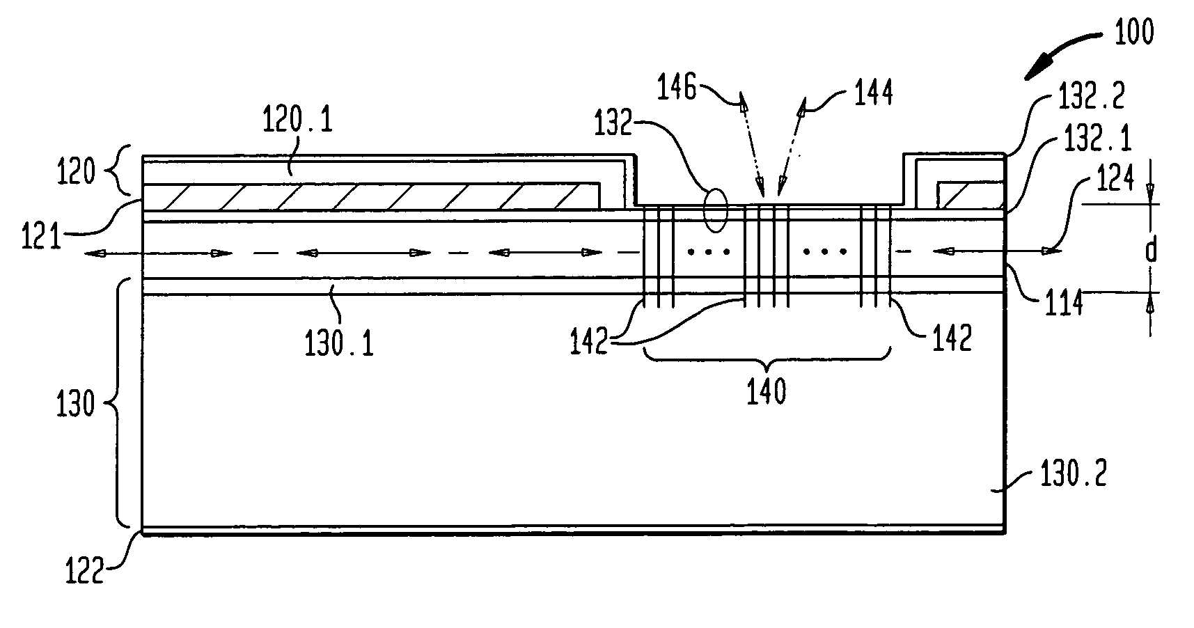
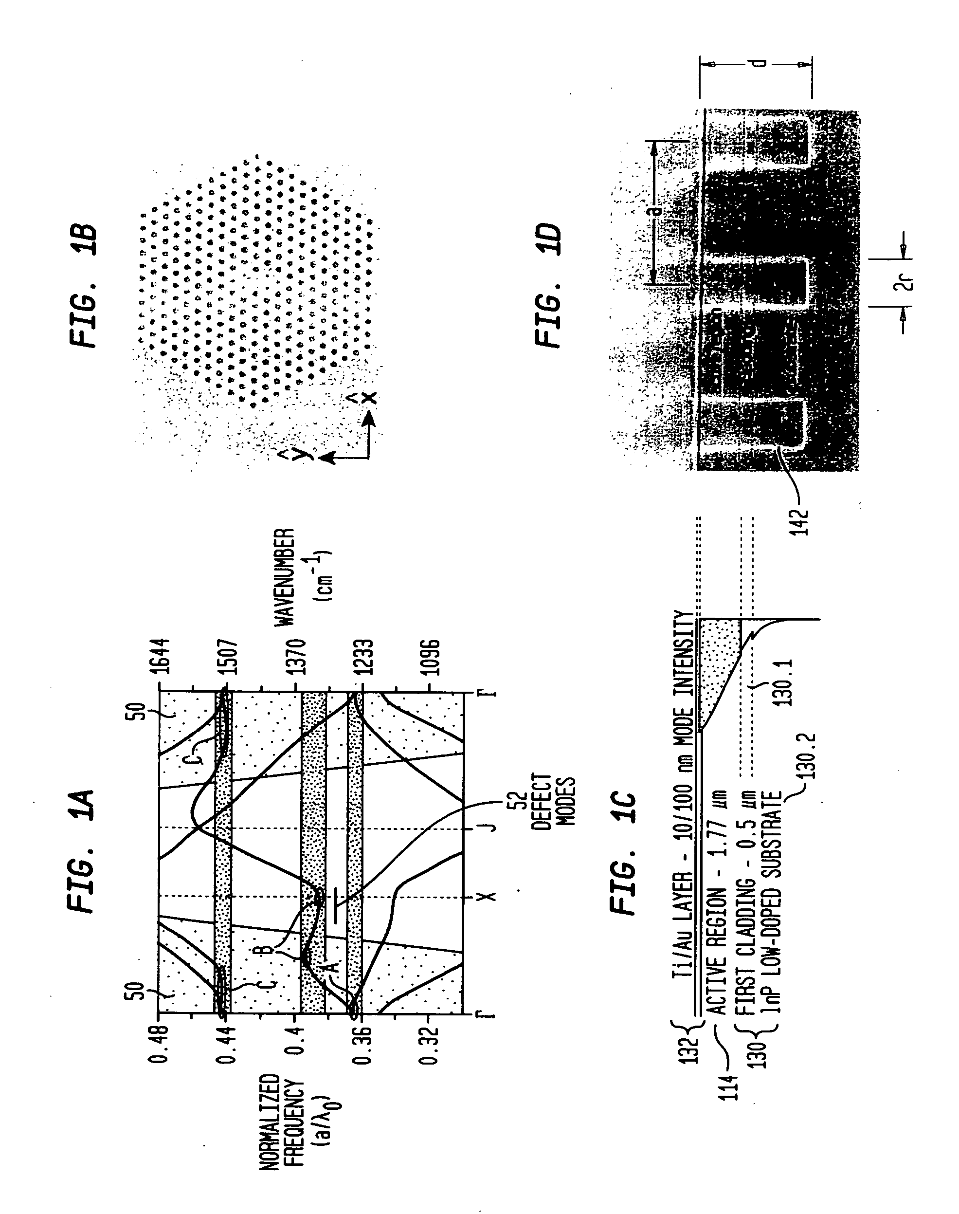
[0066] In this example, the micro-cavity resonator was formed by etching essentially equally spaced air holes that penetrated through the core region and extend deep into the lower waveguide cladding. The deep holes, which had a relatively high aspect ratio (d / 2r˜2.5-3.0) were arranged in a hexagonal pattern, altered the photonic density of states in the lower semiconductor cladding, providing efficient vertical optical confinement. [See, B. D'Urso et al, J. Opt. Soc. Am. B, Vol. 15, p. 1155 (1998)], which is incorporated herein by refe...


PUM


Abstract

An optoelectronic transducer comprises a unipolar, intraband active region and a micro-cavity resonator. The resonator includes a 2D array of essentially equally spaced regions that exhibits resonant modes. Each of the spaced regions has a depth that extends through the active region and has an average refractive index that is different from that of the active region. The refractive index contrast, the spacing of the spaced regions, and the dimensions of the spaced regions are mutually adapted so that the array acts as a micro-cavity resonator and so that at least one frequency of the resonant modes of the array falls within the spectrum of an optoelectronic parameter of the active region (i.e., the gain spectrum where the transducer is a laser; the absorption spectrum where the transducer is a photodetector). In a first embodiment, the transducer is an ISB laser, whereas in a second embodiment it is a unipolar, intraband photodetector. In other embodiments, the laser is a surface-emitting ISB laser and the photodetector is a vertically-illuminated detector. In another embodiment, a nonlinear optical material is optically coupled to the micro-cavity resonator, which in one case allows an ISB laser to exhibit bistable operation.

Description

GOVERNMENT CONTRACT [0001] This invention was made with Government support under Contract No. DAAD19-00-C-0096 by the DARPA / US Army Research Office. The Government has certain rights in this invention.BACKGROUND OF THE INVENTION [0002] 1. Field of the Invention [0003] This invention relates to unipolar, intraband optoelectronic transducers in general and, more particularly, to intersubband (ISB) semiconductor lasers and intraband photodetectors that include micro-cavity resonators. [0004] 2. Discussion of the Related Art [0005] Optoelectronic transducers convert optical energy to electrical energy (e.g., a photodetector) or they convert electrical energy to optical energy (e.g., a laser). When the active regions of these devices are made from semiconductor materials, they may be either bipolar (e.g., conventional interband photodiodes or laser diodes) or unipolar (e.g., conventional ISB lasers or intraband quantum well infrared photodetectors, known as QWIPs). [0006] We focus here o...

Claims


Application Information

Patent Timeline
Patent Type & Authority Applications(United States)
IPC IPC(8): H01S5/00H01S5/10H01S5/187H01S5/32H01S5/34H01S5/40H01S5/42
CPCB82Y20/00H01S5/1042H01S5/105H01S5/187H01S2302/02H01S5/3422H01S5/4087H01S5/42H01S5/3213H01S5/11
Inventor CAPASSO, FEDERICOCHO, ALFRED YICOLOMBELLI, RAFFAELEGMACHL, CLAIRE F.PAINTER, OSKAR JONSERGENT, ARTHUR MIKESIVCO, DEBORAH LEESRINIVASAN, KARTIKTENNANT, DONALD MILANTROCCOLI, MARIANO
Owner ALCATEL-LUCENT USA INC
Why Eureka
Try Eureka