Reduced footprint tool for automated processing of microelectronic substrates

Inactive Publication Date: 2005-03-24
FSI INTERNATIONAL INC
View PDF26 Cites 30 Cited by
  • Summary
  • Abstract
  • Description
  • Claims
  • Application Information

AI Technical Summary

Benefits of technology

[0008] The present invention provides tools and methods of processing microelectronic substrates in which the tools maintain high throughput yet have dramatically lower footprint than conv

Problems solved by technology

The production capacity of a fabrication facility is generally limited by the amount of useable manufacturing space in the fabrication facility.
It is gene

Method used


Image

  • Reduced footprint tool for automated processing of microelectronic substrates
  • Reduced footprint tool for automated processing of microelectronic substrates
  • Reduced footprint tool for automated processing of microelectronic substrates

Examples


Embodiment Construction

[0025] The embodiments of the present invention described below are not intended to be exhaustive or to limit the invention to the precise forms disclosed in the following detailed description. Rather the embodiments are chosen and described so that others skilled in the art may appreciate and understand the principles and practices of the present invention.

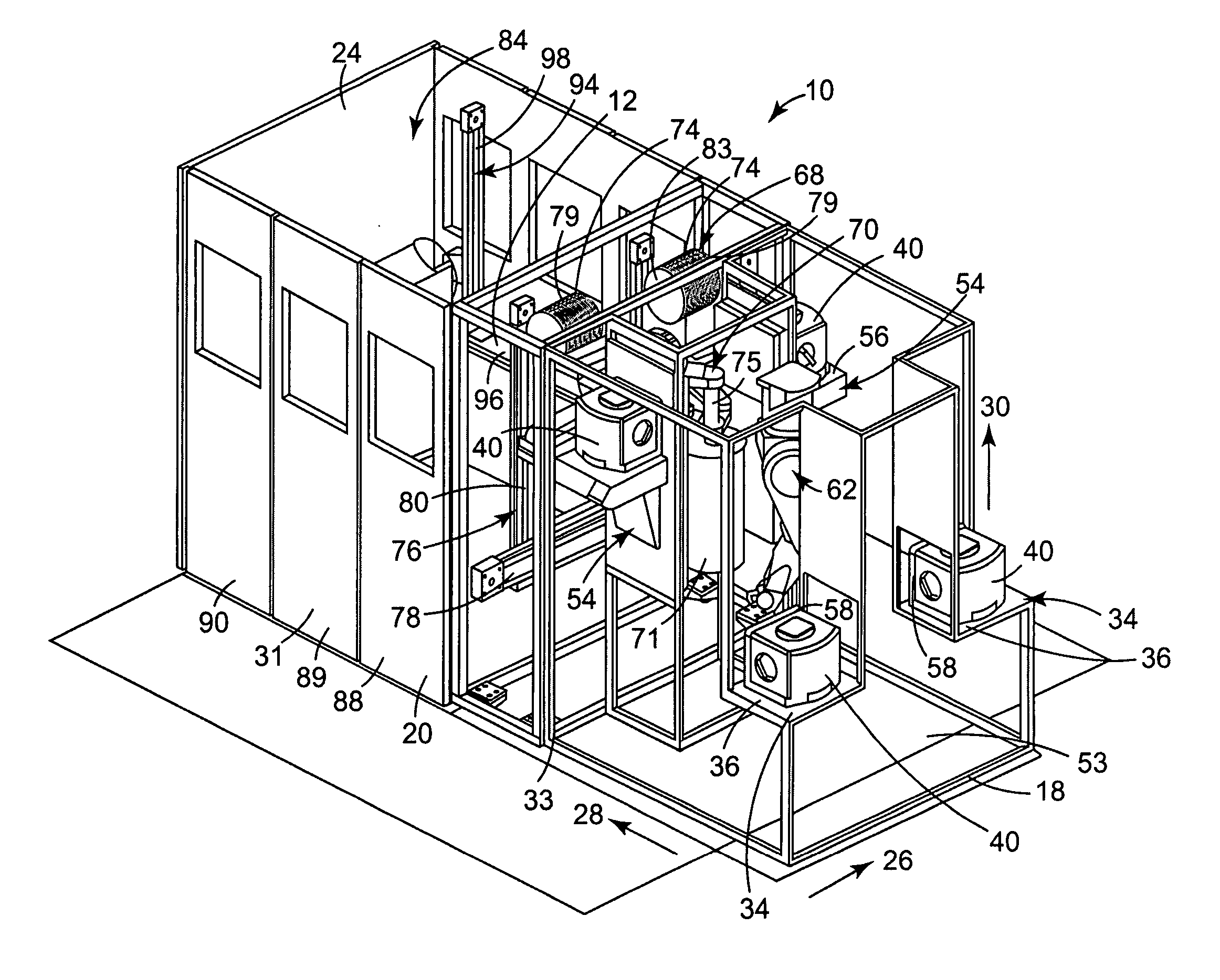
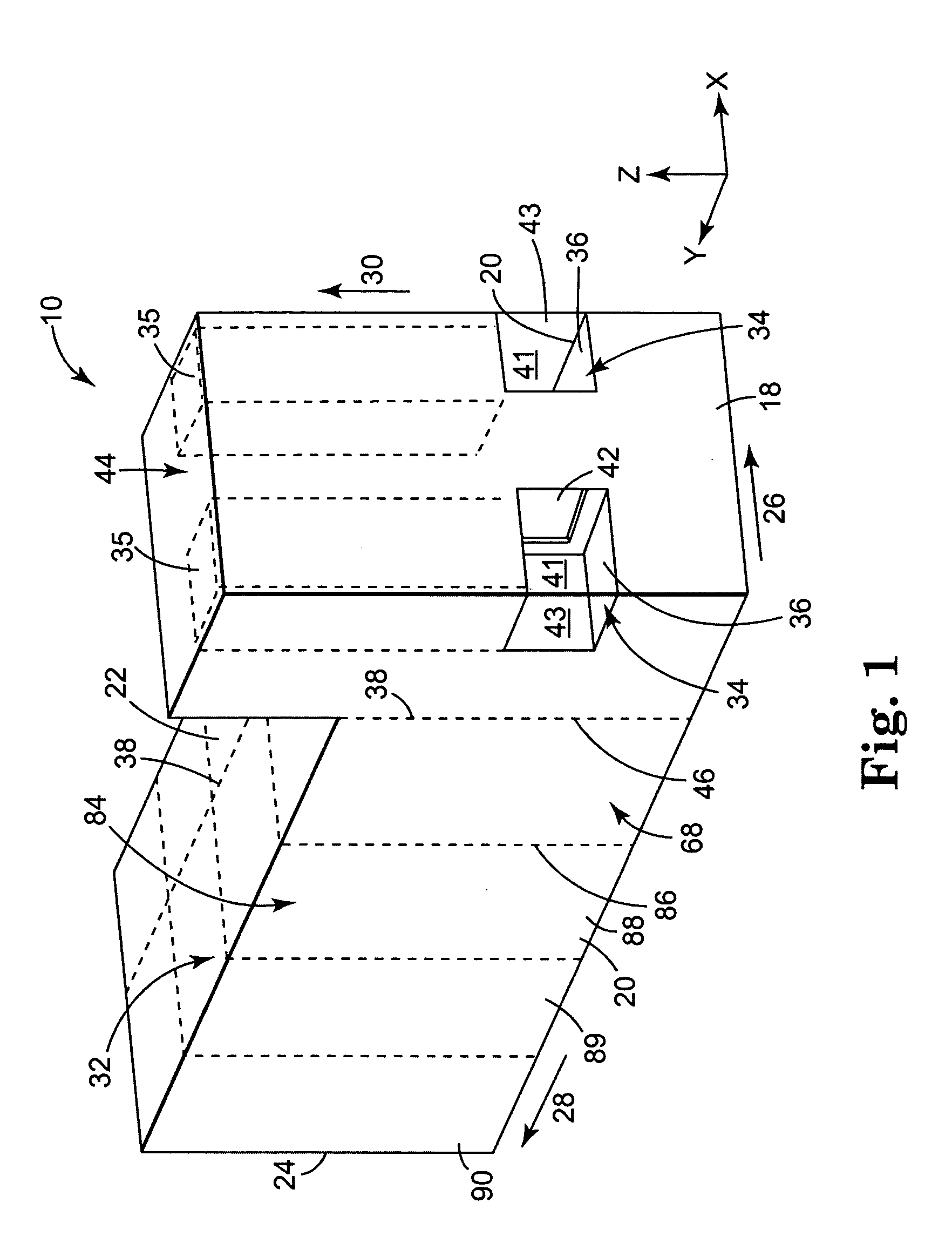
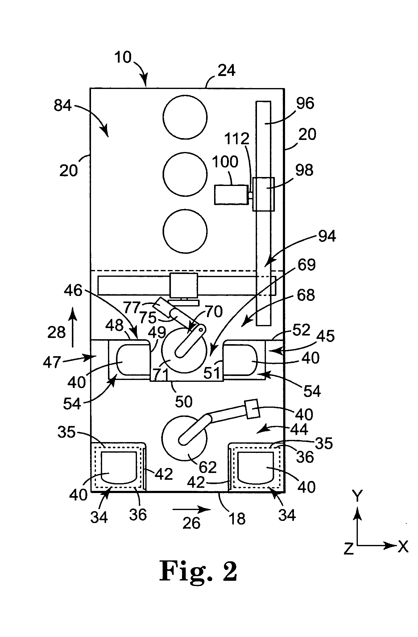
[0026] A representative embodiment of a process tool 10 incorporating the principles of the present invention is shown in FIGS. 1 through 11. Process tool 10 of the invention includes housing 32 having a front side 18, sides 20, top 22, and rear 24. Housing 32 is formed from componentry including panels 31 and an underlying, supportive framework 33. Tool 10 has a width that extends along x-axis direction 26, a height that extends along z-axis direction 30; and a length that extends along y-axis direction 28. The front side 18 of tool 10 is provided with one or more interfaces through which batches of processable microelectronic ...


PUM


Abstract

The present invention provides tools and methods of processing microelectronic substrates in which the tools maintain high throughput yet have dramatically lower footprint than conventional tools. In preferred aspects, the present invention provides novel tool designs in which multiple tool functions are overlapped in the x, y, and/or z axes of the tool in novel ways.

Description

CROSS-REFERENCE TO RELATED APPLICATIONS [0001] This divisional patent application is entitled to the benefit of priority, under 35 U.S.C. §§ 120 and 121, of the filing date of commonly owned U.S. Nonprovisional Patent Application No. 10 / 292,147, filed Nov. 12, 2002, and titled REDUCED FOOTPRINT TOOL FOR AUTOMATED PROCESSING OF MICROELECTRONIC SUBSTRATES, the entire contents of which are incorporated herein by reference, which in turn is entitled to the benefit of priority, under 35 U.S.C. §119(e), of the filing date of commonly owned U.S. Provisional Patent Application No. 60 / 338,057, filed Nov. 13, 2001, and titled REDUCED FOOTPRINT TOOL FOR AUTOMATED PROCESSING OF MICROELECTRONIC SUBSTRATES, the entire contents of which are incorporated herein by reference.FIELD OF THE INVENTION [0002] The present invention relates to automated tools used in the manufacture of microelectronic devices. More specifically, the present invention relates to such tools that incorporate tool architecture...

Claims


Application Information

Patent Timeline
IPC IPC(8): B65G49/07H01L21/00H01L21/02H01L21/304H01L21/677
CPCH01L21/67161H01L21/67167H01L21/67173H01L21/67178Y10S414/139H01L21/67769H01L21/67781Y10S414/138Y10S414/141H01L21/67196H01L21/00
Inventor LARSON, ROBERT E.SIMONDET, SEAN D.ZIMMERMAN, DAVID C.MACIEJ, TODD K.MATTHYS, QUIRIN W.
Owner FSI INTERNATIONAL INC
Why Eureka
Try Eureka