Methods of and laser systems for link processing using laser pulses with specially tailored power profiles

a laser system and laser technology, applied in wavelength-division multiplex systems, semiconductor/solid-state device details, manufacturing tools, etc., can solve the problems of ever-shrinking link dimensions, imposing a great risk of damaging the silicon substrate, and small laser beams, so as to improve the processing quality of removal

Active Publication Date: 2005-03-31
ELECTRO SCI IND INC
View PDF42 Cites 85 Cited by
  • Summary
  • Abstract
  • Description
  • Claims
  • Application Information

AI Technical Summary

Benefits of technology

[0014] An object of the present invention is to provide a method of and an apparatus for improving the processing quality of removal of IC link and overlying passivation structure material fabricated on a substrate.
[0015] Another object of the invention is to process a link with a specially tailored temporal laser pulse power profile to achieve improved process quality and a wider process window.
[0016] A further object of the invention is to provide a method of and an apparatus for employing a smaller laser beam spot size for link removal techniques with a shorter laser wavelength without appreciable damage to the substrate and side and underlying passivation structure material surrounding the link being removed.
[0018] The specially tailored laser pulse power profile allows the use of a wider laser pulse energy range and shorter laser wavelengths, such as green and UV to generate an opening in the overlying passivation layer and sever the links. The opening is sufficiently wide to accomplish severing the link but sufficiently narrow to not appreciably damage any neighboring structures. The technique does not appreciably damage the substrate and the passivation structure material located on either side of and underlying the link as well.
[0021] In a further embodiment, a laser output pulse emitted from a diode laser is injected into a power amplifier. The temporal power profile of the laser pulse emitted from the diode laser is specially tailored by controlling its driver. The power amplifier operates in an unsaturated state to provide an amplified laser output pulse that substantially replicates the specially tailored temporal power profile of the injected laser pulse and to deliver adequate laser energy within the pulse for the link processing applications. Persons skilled in the art will appreciate that they could readily accomplish tailoring of the temporal current profile of the drive pulse from the diode laser driver to generate the laser pulse emitted from the diode laser characterized by the specially tailored power profile preferred for the link process application.

Problems solved by technology

However, ever-shrinking link dimensions and link-to-link pitch sizes demand a smaller laser beam spot size.
However, expose and etch removal techniques employ additional coating, developing, and / or etching steps, which typically entail sending the wafer back to the front end of the manufacturing process for one or more extra steps.
Persons skilled in the art will realize that the laser pulse energy after time t1 for both cases imposes a great risk of damaging the silicon substrate because there would be no link material remaining to shield the substrate from exposure to the laser energy.
The laser pulse energy after time t1 imposes great risk of damaging also the neighboring structure to the link.
Unfortunately, for the traditional laser pulse, there is no control over the temporal shape of the laser pulse after time t1.
For the substantially square temporal laser pulse, it is worse in that right after the time t1 the laser pulse will remain at its peak intensity for a while, causing even greater risk of damage to the substrate or neighboring structure.

Method used


Image

  • Methods of and laser systems for link processing using laser pulses with specially tailored power profiles
  • Methods of and laser systems for link processing using laser pulses with specially tailored power profiles
  • Methods of and laser systems for link processing using laser pulses with specially tailored power profiles

Examples


first embodiment

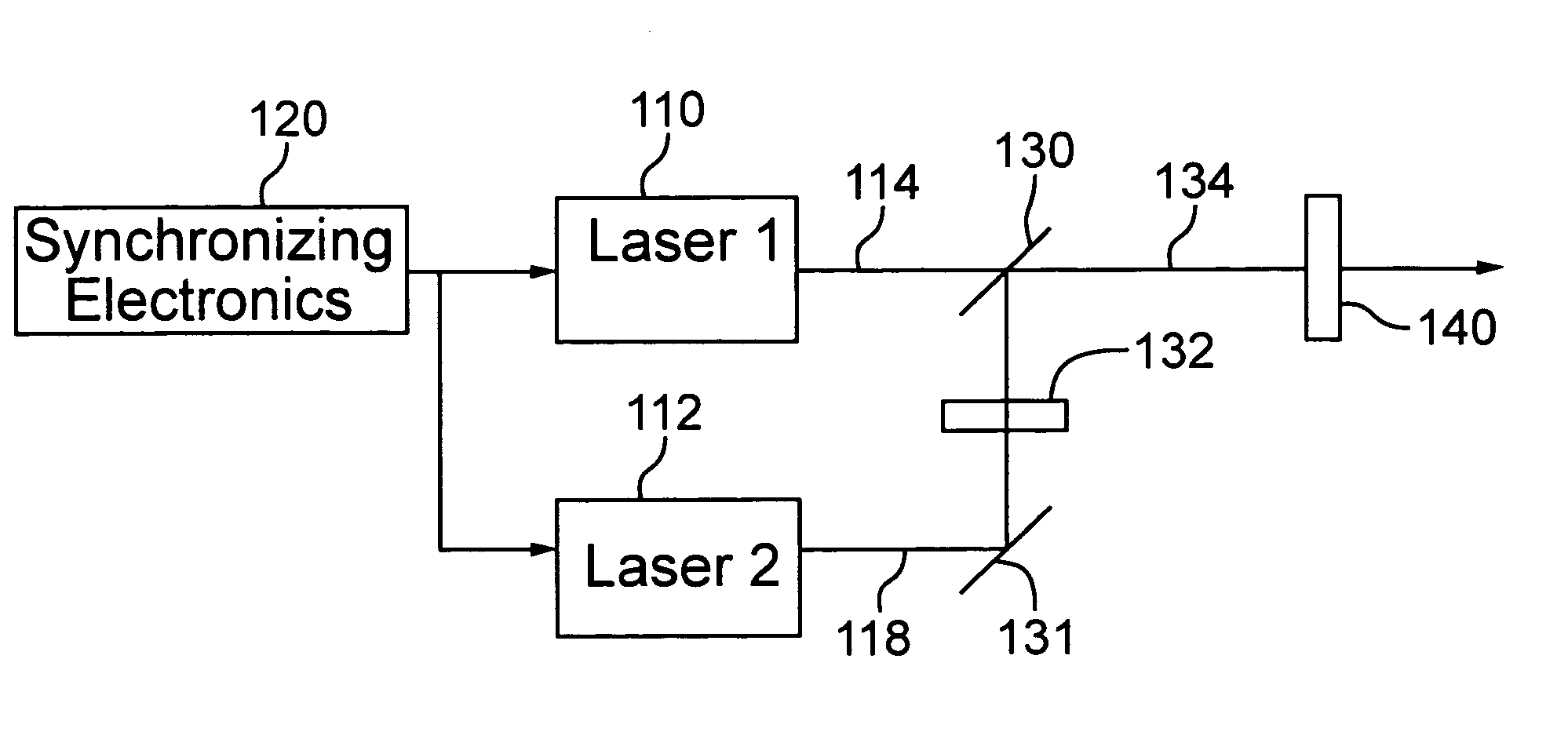
[0043] With reference to FIG. 4A, in a first embodiment, special tailoring of the laser pulse power profile is accomplished by combining two laser pulses from two separate laser rails 110 and 112. Laser rail 110 generates a shorter laser pulse 114, shown in FIG. 4B, and laser rail 112 generates a longer laser pulse 118, shown in FIG. 4C. The synchronization of or delay time (td) between laser pulses 114 and 118 is controlled by synchronizing electronics 120. Laser pulses 114 and 118 are combined by a beam combiner 130 after laser pulse 118 reflects off a mirror 131 and propagates through a waveplate 132 for polarization control purposes. FIG. 4D shows a combined laser pulse 134 that has a final power profile with a significant power spike 136 preferred for link processing. The total laser pulse width of combined laser pulse 134 can be either the sum of the widths of laser pulses 114 and 118 or the width of laser pulse 118, depending on the delay time between laser pulses 114 and 118...

second embodiment

[0046] With reference to FIG. 5A, in a second embodiment, an E-O gating device 150 shapes the power profile of laser pulses propagating from a diode-pumped, Q-switched solid state laser 152. Laser 152 delivers multiple laser pulses 160 (one shown in FIG. 5B), each with a relatively long laser pulse width at full width, half maximum (FWHM). The FWHM pulse width can be, for example, about 30 ns to 50 ns. Laser pulses 160 propagate through E-O gating device 150. The output laser pulse power profile depends on the width and shape of a drive voltage pulse 162 delivered from drive electronics 164 and the delay time between laser pulse 160 and the drive voltage pulse 162 applied to E-O device 150. The output laser pulse can have an upwardly, substantially linearly inclined (increasing) power profile, as shown for laser pulse 166c in FIG. 5C or a downwardly, substantially linearly inclined (decreasing) power profile with a higher peak at the very beginning of the laser pulse, as shown for l...

third embodiment

[0047] With reference to FIG. 6A, in a third embodiment, a laser 200 is composed of an injection laser 202 followed by an amplifier 204. Injection laser 202 can be a diode laser having a fast response time and delivering laser output at a laser wavelength that matches the gain spectrum of amplifier 204. FIG. 6B shows a specially tailored drive current pulse 206 delivered from driving electronics 208, and FIG. 6C shows that an injection laser output pulse 210 propagating from injection laser 202 replicates the profile of drive current pulse 206 as a result of the fast response capability of injection laser 202. Injection laser output pulse 210 is delivered to laser power amplifier 204, which is operating in an unsaturated state to amplify injection laser output pulse 210 and deliver an output pulse 212 without introducing significant distortion of the tailored laser pulse power profile, as shown in FIG. 6D. Output pulse 212 is relatively flat after the occurrence of the power spike a...


PUM

PropertyMeasurementUnit
rise timeaaaaaaaaaa
rise timeaaaaaaaaaa
laser energyaaaaaaaaaa

Abstract

A laser pulse with a specially tailored temporal power profile, instead of a conventional temporal shape or substantially square shape, severs an IC link. The specially tailored laser pulse preferably has either an overshoot at the beginning of the laser pulse or a spike peak within the duration of the laser pulse. The timing of the spike peak is preferably set ahead of the time when the link is mostly removed. A specially tailored laser pulse power profile allows the use of a wider laser pulse energy range and shorter laser wavelengths, such as the green and UV, to sever the links without appreciable damage to the substrate and passivation structure material located on either side of and underlying the links.

Description

RELATED APPLICATION [0001] This application claims benefit of U.S. Provisional Patent Application No. 60 / 496,631, filed Aug. 19, 2003.COPYRIGHT NOTICE [0002] 2004 Electro Scientific Industries, Inc. A portion of the disclosure of this patent document contains material which is subject to copyright protection. The copyright owner has no objection to the facsimile reproduction by anyone of the patent document or the patent disclosure, as it appears in the Patent and Trademark Office patent file or records, but otherwise reserves all copyright rights whatsoever. 37 CFR § 1.71(d). TECHNICAL FIELD [0003] The present invention relates to laser processing of conductive links on memory chips or other integrated circuit (IC) chips and, in particular, to laser methods and systems employing laser pulses having specially tailored power profiles for better processing quality and yield. BACKGROUND OF THE INVENTION [0004] Decreased yields in IC device fabrication processes often result from defect...

Claims


Application Information

Patent Timeline
Patent Type & Authority Applications(United States)
IPC IPC(8): B23KB23K26/06B23K26/38H01SH04J14/02
CPCB23K26/0613B23K26/063B23K2201/40H01L23/5258H01L2924/0002H01L2924/00B23K26/0622B23K2101/40B23K26/00H01S3/10007H01S3/101B23K26/0608
Inventor SUN, YUNLONGHARRIS, RICHARDLO, HO WAIBAIRD, BRIANJOHNSON, JAY
Owner ELECTRO SCI IND INC
Why Eureka
Try Eureka