Analog-to-digital converter having cyclic configuration

a technology of analog-to-digital converter and configuration, which is applied in the field of analog-to-digital converter technology of cyclic, can solve the problems of increasing power consumption, securing excessive conversion processing speed and conversion accuracy, and reducing the power consumption of ad converters, so as to reduce the power consumption and optimize the conversion accuracy

Active Publication Date: 2005-03-31
SEMICON COMPONENTS IND LLC
View PDF6 Cites 14 Cited by
  • Summary
  • Abstract
  • Description
  • Claims
  • Application Information

AI Technical Summary

Benefits of technology

[0040] According to the present invention, it is possible to optimize the

Problems solved by technology
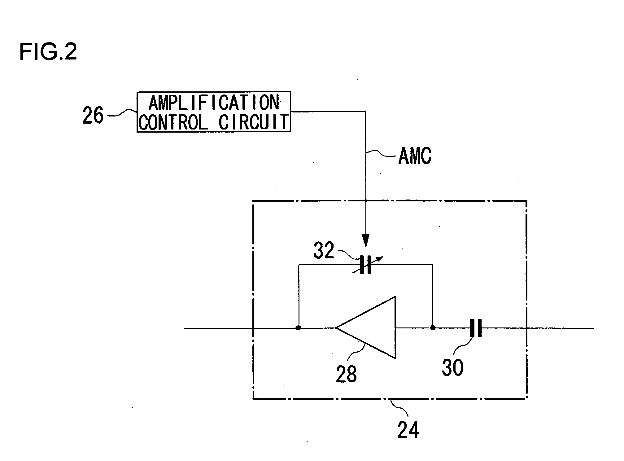
This means that the conversion processing speed and conversion accuracy to be secured can sometimes be excessive to the entire process of the cyclic processing.
Besides, securing excessive conversion processing speed and conversion accuracy throughout all the stages of the cyclic proc

Method used


Image

  • Analog-to-digital converter having cyclic configuration
  • Analog-to-digital converter having cyclic configuration
  • Analog-to-digital converter having cyclic configuration

Examples


first embodiment

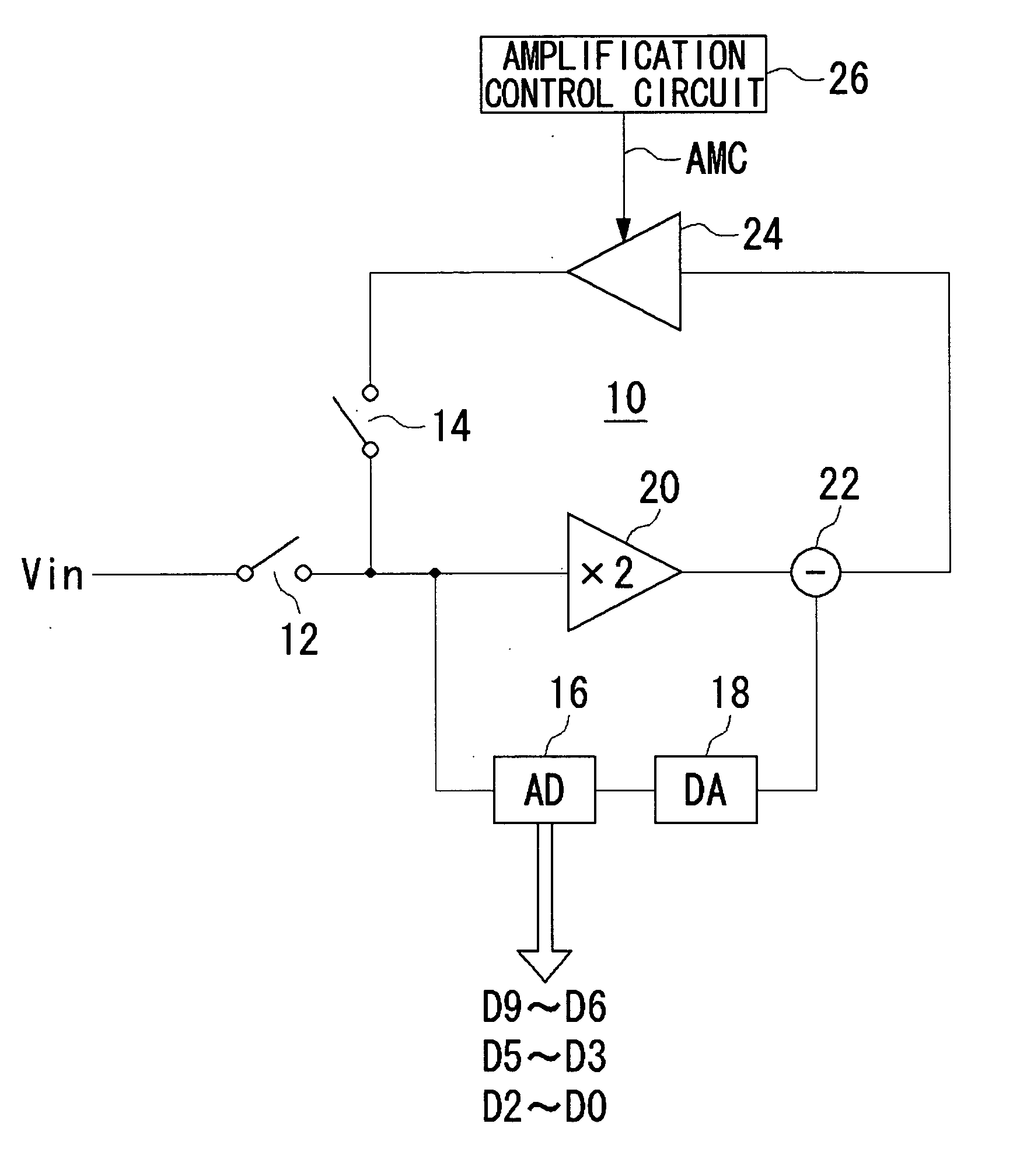
[0105] In the present embodiment, the reference voltage range for generating reference voltages of the AD conversion circuit included in an AD converter of cyclic type is changed in accordance with the progress of the cyclic processing. Specifically, the reference voltage range mentioned above is reduced by half at the second and subsequent cycles. This makes it possible to suppress the gain of the amplifier circuit, allowing speedup of the entire AD converter.

[0106]FIG. 14 shows the configuration of the AD converter according to a first embodiment of the second group. In the AD converter, an input analog signal Vin is input to a first amplifier circuit 1011 and an AD conversion circuit 1012 through a first switch SW101. The AD conversion circuit 1012 converts the input analog signal into a maximum of four bits of digital value, and outputs the same to a not-shown encoder and a DA conversion circuit 1013. The DA conversion circuit 1013 converts the 4-bit maximum digital value outpu...

second embodiment

[0129] In the present embodiment, the first amplifier circuit is given a gain of 2 and the second amplifier circuit a gain of 2 while the amplifier circuit 1011 according to the first embodiment of the second group has a gain of 1 and the second amplifier circuit 1015 a gain of 4. This allows speedup further than in the first embodiment of the second group.

[0130]FIG. 20 shows the configuration of the AD converter according to the second embodiment of the second group. In the AD converter, an input analog signal Vin is input to a first amplifier circuit 1011 and an AD conversion circuit 1012 through a first switch SW101. The AD conversion circuit 1012 converts the input analog signal into a maximum of four bits of digital value, and outputs the same to a not-shown encoder and a DA conversion circuit 1013. The DA conversion circuit 1013 converts the 4-bit maximum digital value output from the AD conversion circuit 1012 into an analog signal.

[0131] The first amplifier circuit 1011 sa...

third embodiment

[0156] A third embodiment of the second group provides a cyclic AD converter having the configuration of changing the reference voltages of the AD conversion circuit 1012 and the gain of the first amplifier circuit 1011 as well.

[0157]FIG. 22a shows the configuration of the AD converter at its first cycle according to the third embodiment of the second group. FIG. 22b shows the configuration of the AD converter at the second and subsequent cycles according to the second embodiment of the second group. In the AD converter, an input analog signal Vin is input to a first amplifier circuit 1011 and an AD conversion circuit 1012 through a first switch SW101. The AD conversion circuit 1012 converts the input analog signal into a maximum of four bits of digital value, and outputs the same to a not-shown encoder and a DA conversion circuit 1013. The DA conversion circuit 1013 converts the 4-bit maximum digital value output from the AD conversion circuit 1012 into an analog signal.

[0158] Th...


PUM


Abstract

A cyclic AD converter having a conversion processing speed or conversion accuracy designed no higher than necessary. In the AD converter, an input analog signal is held by a sample-and-hold circuit, and converted into a digital value by an AD conversion circuit. A DA conversion circuit converts the digital value output from the AD conversion circuit into an analog value. A subtractor circuit outputs the difference between the analog value output from the AD conversion circuit and the analog value held in the sample-and-hold circuit. An amplifier circuit amplifies the output of the subtractor circuit, and feeds back the resultant to the sample-and-hold circuit and the AD conversion circuit. In the course of this feedback-based cyclic processing, an amplification control circuit changes the gain of the amplifier circuit in accordance with the progress of the circulation.

Description

BACKGROUND OF THE INVENTION [0001] 1. Field of the Invention [0002] The present invention relates to an analog-to-digital converter. In particular, the invention relates to analog-to-digital conversion technologies of cyclic type. [0003] 2. Description of the Related Art [0004] (First Related Art) [0005] Recently, cellular phones have incorporated a variety of additional functions such as an image capturing function, an image reproducing function, a moving image capturing function, and a moving image reproducing function. Reduced size and reduced power consumption are thus increasingly required of analog-to-digital converters (hereinafter, referred to as “AD converters”). One of the known forms of such AD converters is a cyclic AD converter which has a cyclic configuration (for example, see Japanese Patent Laid-Open Publication No. Hei 11-145830). FIG. 13 shows the configuration of a conventional cyclic AD converter. In this AD converter 150, an analog signal Vin input through a fir...

Claims


Application Information

Patent Timeline
IPC IPC(8): H03F1/00H03M1/06H03M1/12H03M1/14H03M1/16H03M1/36H03M1/38H03M1/40
CPCH03M1/06H03M1/365H03M1/162
Inventor KOBAYASHI, SHIGETOTANI, KUNIYUKIWADA, ATSUSHINAKAMORI, TAKAFUMI
Owner SEMICON COMPONENTS IND LLC
Why Eureka
Try Eureka