Monolithic semiconductor laser and method of manufacturing the same

a semiconductor laser and monolithic technology, applied in the direction of semiconductor lasers, semiconductor laser arrangements, active medium materials, etc., can solve the problems of increasing manufacturing costs and complex assembly steps, and achieve the effect of increasing manufacturing costs

Inactive Publication Date: 2005-03-31
MITSUBISHI ELECTRIC CORP
View PDF20 Cites 15 Cited by
  • Summary
  • Abstract
  • Description
  • Claims
  • Application Information

AI Technical Summary

Benefits of technology

[0009] The fine adjustment makes the assembling step complex and increases a manufacturing cost.

Problems solved by technology

The fine adjustment makes the assembling step complex and increases a manufacturing cost.

Method used


Image

  • Monolithic semiconductor laser and method of manufacturing the same
  • Monolithic semiconductor laser and method of manufacturing the same
  • Monolithic semiconductor laser and method of manufacturing the same

Examples


embodiment 1

[0019] Embodiment 1

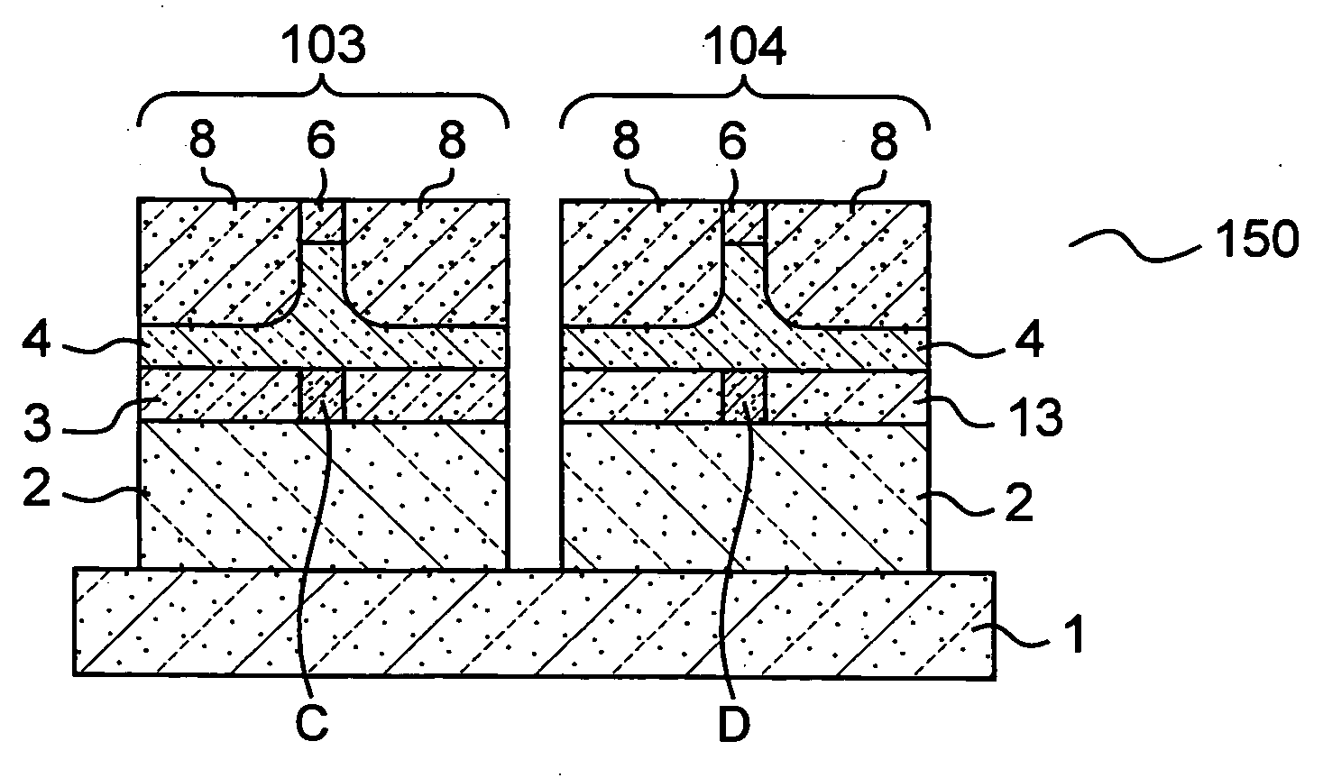
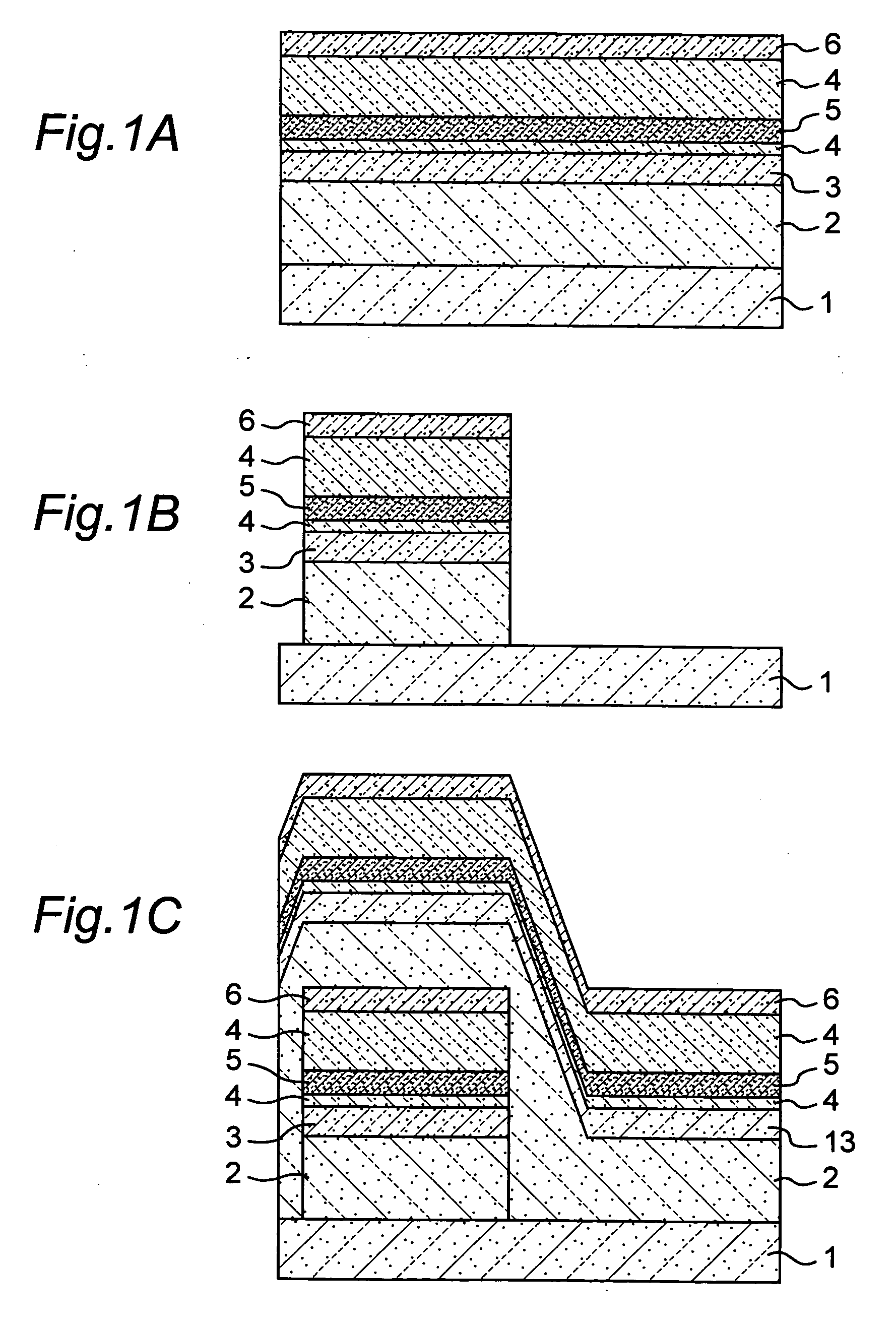
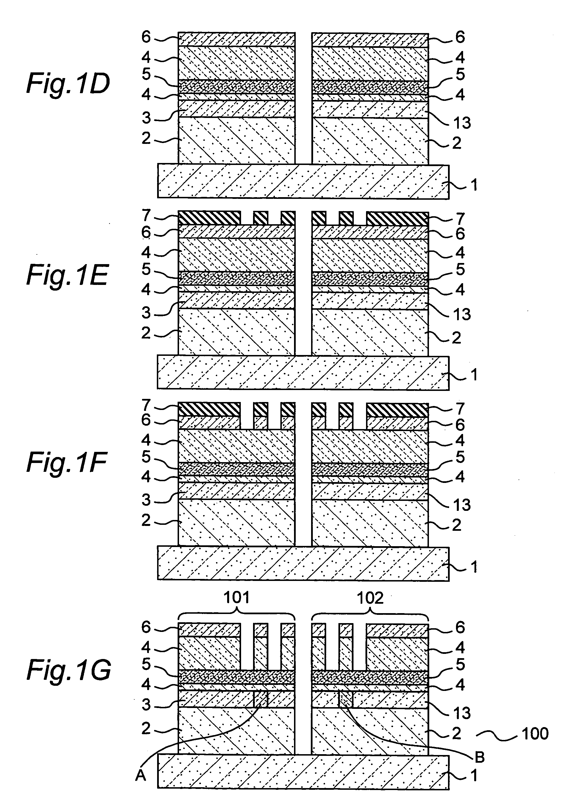
[0020]FIGS. 1A-1G are cross sectional views of steps of manufacturing a monolithic semiconductor laser according to this embodiment which is generally denoted at 100. The monolithic semiconductor laser 100 has a first semiconductor laser whose emission wavelength is 780 nm and a second semiconductor laser whose emission wavelength is 650 nm (See FIG. 1G).

[0021] The steps of manufacturing the monolithic semiconductor laser 100 will now be described with reference to FIGS. 1A-1G. These steps include the following steps 1 through 7.

[0022] Step 1: As shown in FIG. 1A, a GaAs substrate 1 of the n-type is prepared. On the GaAs substrate 1, an n-AlGaInP lower clad layer 2, an AlGaAs active layer (having the emission wavelength of 780 nm) 3 and a p-AlGaInP upper clad layer 4 are then stacked one atop the other. A GaInP etching stopper layer 5 is inserted in the p-AlGaInP upper clad layer 4. Further, on the p-AlGaInP upper clad layer 4, a p-GaAs cap layer 6 is formed.

[0...

embodiment 2

[0049] Embodiment 2

[0050]FIGS. 2A-2C show cross sectional views of steps of manufacturing a monolithic semiconductor laser according to this embodiment which is generally denoted at 200. The monolithic semiconductor laser 200 has two semiconductor lasers 201 and 202 which have different emission wavelengths (The emission wavelengths are 780 nm and 650 nm for example.) (FIG. 2C).

[0051] In the monolithic semiconductor laser 200 according to the embodiment 2, the compositions and the like of other layers than active layers are different between the two semiconductor lasers 201 and 202. Use of stopper layers makes it possible to etch at a high accuracy also in these structures.

[0052] Through approximately the same steps (FIGS. 1A-1D) as those exercised in the embodiment 1 described above, a stacked structure as that shown in FIG. 2A is fabricated on an n-GaAs substrate 1.

[0053] As the first semiconductor laser, on the n-GaAs substrate 1, an n-AlGaInP lower clad layer 21, an AlGaAs ac...

embodiment 3

[0068] Embodiment 3

[0069]FIGS. 3A-3C show cross sectional views of steps of manufacturing a monolithic semiconductor laser according to this embodiment which is generally denoted at 300. The monolithic semiconductor laser 300 comprises two semiconductor lasers 301 and 302 which have different emission wavelengths (The emission wavelengths are 780 nm and 650 nm for example.) (FIG. 3C).

[0070] In the monolithic semiconductor laser 300, ridge-type stripes are formed so that the ridge-type stripes have different depths between the two semiconductor lasers 301 and 302, and the refractive indices of the ridge-type stripes are adjusted.

[0071] In the monolithic semiconductor laser 300, first, through approximately the same steps (FIGS. 1A-1D) as those exercised in the embodiment 1 described earlier, a stacked structure as that shown in FIG. 3A is fabricated on an n-GaAs substrate 1.

[0072] As the first semiconductor laser, on the n-GaAs substrate 1, an n-AlGaInP lower clad layer 41, an AlG...


PUM


Abstract

A monolithic semiconductor laser having plural semiconductor lasers having different emission wavelengths from each other, including: a semiconductor substrate; a first double hetero-structure formed within a first area on the semiconductor substrate and having first clad layers disposed above and below a first active layer; and a second double hetero-structure formed within a second area on the semiconductor substrate and having second clad layers disposed above and below a second active layer. The first and second active layers are made of different semiconductor materials from each other. The first clad layers above and below the first active layer are of approximately the same semiconductor materials and the second clad layers above and below the second active layer are of approximately the same semiconductor materials.

Description

CROSS-REFERENCE TO RELATED APPLICATION [0001] Related patent application is commonly assigned Japanese Patent Application No. 2003-339768 filed on Sep. 30, 2003, which is incorporated by reference into the present patent application. BACKGROUND OF THE INVENTION [0002] 1. Field of the Invention [0003] The present invention relates to a monolithic semiconductor laser and a method of manufacturing the same, and more particularly, to a monolithic semiconductor laser comprising a stripe structure (current confining structure) and a method of manufacturing the same. [0004] 2. Description of the Related Art [0005] An information reader / writer apparatus or the like for DVDs and CDs uses a monolithic semiconductor laser in which the single substrate seats multiple of semiconductor lasers which have different emission wavelengths. In such a monolithic semiconductor laser, the single substrate seats a semiconductor laser whose emission wavelength is 650 nm and a semiconductor laser whose emiss...

Claims


Application Information

Patent Timeline
Patent Type & Authority Applications(United States)
IPC IPC(8): H01S5/22H01S5/20H01S5/223H01S5/30H01S5/343H01S5/40
CPCB82Y20/00H01S5/2063H01S5/2086H01S5/209H01S5/4087H01S5/34326H01S5/34353H01S5/4031H01S5/2231H01S5/22H01S5/30
Inventor NISHIDA, TAKEHIROMIYASHITA, MOTOHARUYAMAGUCHI, TSUTOMU
Owner MITSUBISHI ELECTRIC CORP
Why Eureka
Try Eureka