Power supply layout for an integrated circuit

a power supply layout and integrated circuit technology, applied in the direction of semiconductor devices, semiconductor/solid-state device details, instruments, etc., can solve the problems of time delay originating from the capacitance and the resistance of the interconnection, voltage drop that decreases the real voltage supplied, high-performance circuits, etc., to simplify the design work of the integrated circuit

Inactive Publication Date: 2005-03-31
GOYATEK TECH
View PDF6 Cites 11 Cited by
  • Summary
  • Abstract
  • Description
  • Claims
  • Application Information

AI Technical Summary

Benefits of technology

[0019] 4. Since the present invention does not use the power ring, it is no longer necessary to consider the power consumption and electron migration effect during the design of the power suppler layout. Therefore, the design work of the integrated circuit can be simplified.

Problems solved by technology

As the size of the interconnections shrink, the time delay originating from the capacitance and the resistance of the interconnections will increase, which is an obstacle for high performance circuits.
The resistance of the interconnection and the current passing therethrough results in a voltage drop that decreases the real voltage supplied to a core circuit.

Method used


Image

  • Power supply layout for an integrated circuit
  • Power supply layout for an integrated circuit
  • Power supply layout for an integrated circuit

Examples


first embodiment

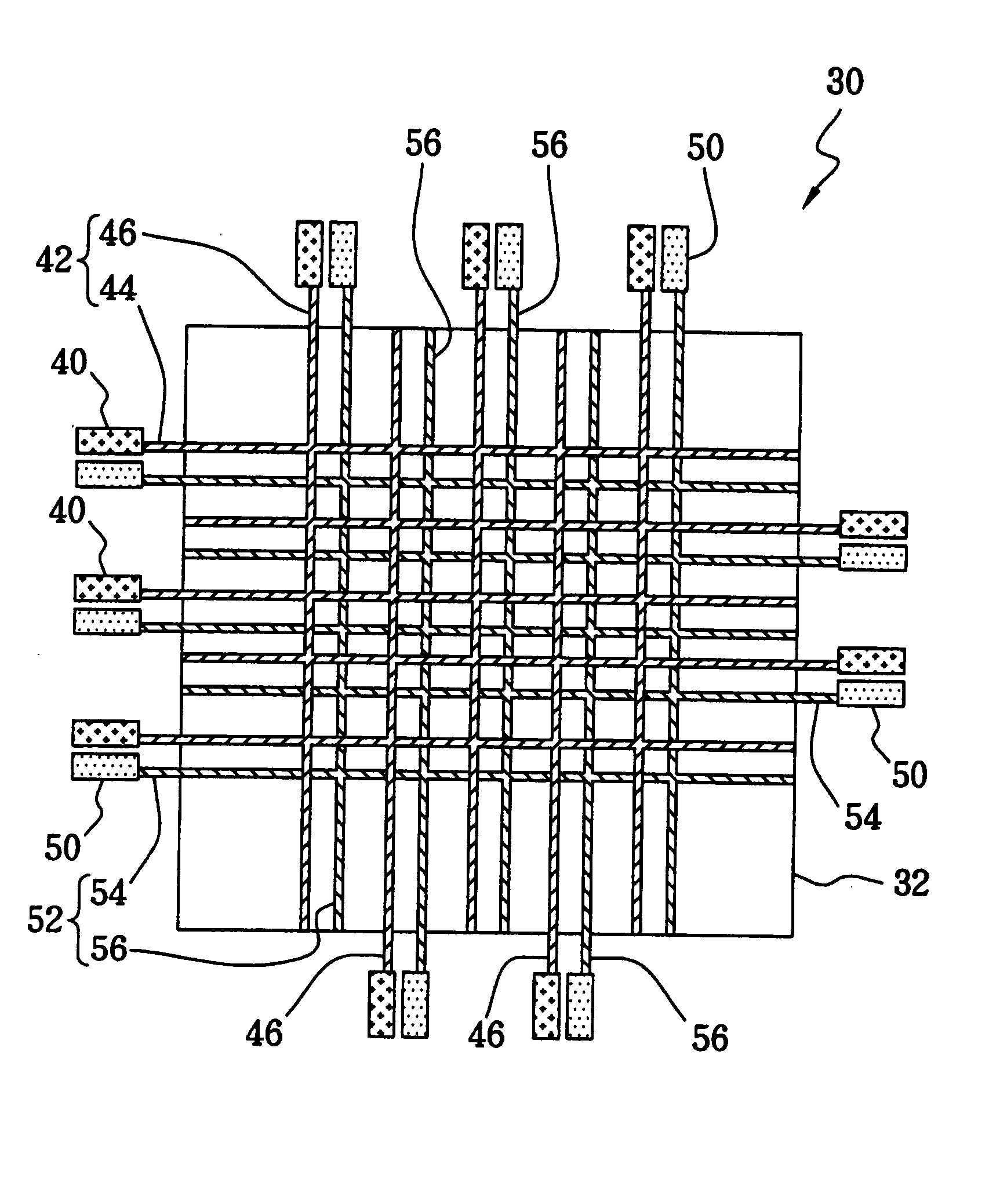
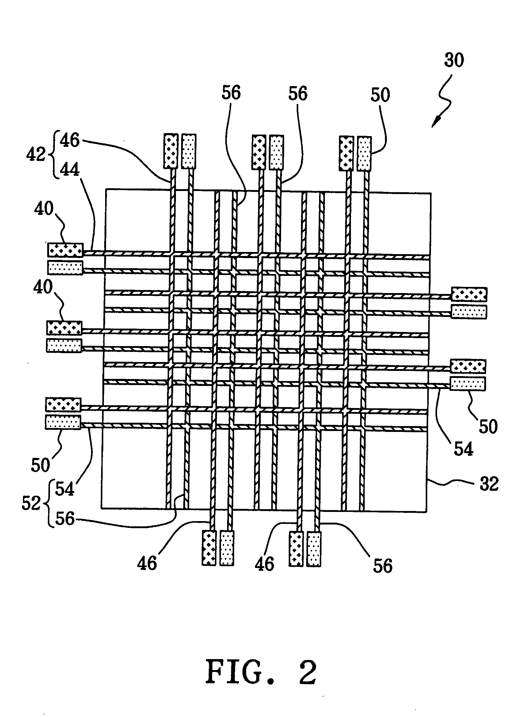
[0025]FIG. 2 is a schematic diagram of an integrated circuit 30 according to the present invention. As shown in FIG. 2, the integrated circuit 30 comprises a plurality of power pads 40, a plurality of ground pads 50, a plurality of first-type conductive wires 42 directly connected to the power pad 40, a plurality of second-type conductive wires 52 directly connected to the ground pad 50, and a core circuit 32. The first-type conductive wire 42 is electrically connected to a positive potential, while the second-type conductive wires 52 is electrically connected to a ground potential. The integrated circuit 30 is made of a plurality of metal layers, and the first-type conductive wire 42 and the second-type conductive wire 52 are positioned at different metal layers. The power pad 40 and the first-type conductive wires 42 are positioned at the same metal layer, and the ground pads 50 and the second-type conductive wire 52 are positioned at the same metal layer.

[0026] The electronic com...

second embodiment

[0028]FIG. 3 is a schematic diagram of an integrated circuit 60 according to the present invention. Compared with the integrated circuit 30 in FIG. 2, the first-type conductive wire 42 and the power pad 40 of the integrated circuit 60 are positioned with different pitches between them, and both ends of first-type conductive wire 42 are electrically connected to the power pads 40 positioned around the core circuit 32 directly. Similarly, the second-type conductive wires 52 and the ground pads 50 are positioned with different pitches between them, and both ends of the second-type conductive wires 52 are electrically connected to the ground pads 50 directly.

[0029] If a certain region 62 of the core circuit 32 requires a higher power supply, the designer can arrange the power pads 40 and ground pads 50 more densely around the region 62 than the other regions, i.e., arrange the first-type conductive wires 42 and second-type conductive wires 52 more densely around the region 62. The volta...

third embodiment

[0030]FIG. 4 is a schematic diagram of an integrated circuit 90 according to the present invention. Compared with the integrated circuit 30 in FIG. 2, the integrated circuit 90 further comprises a plurality of first-type auxiliary wires 70, 72 and a plurality of second-type auxiliary wires 80,82. The first-type auxiliary wire 70 is positioned in parallel to the second wire 46, and the first-type auxiliary wire 72 is positioned in parallel to the first conductive wire 44. Neither of the ends of the first-type auxiliary wires 70,72 is connected to the power pad 40, but the first-type auxiliary wires 70,72 are electrically connected to the first wire 44 and the second wire 46, respectively, to maintain the positive potential. Similarly, neither of the ends of the second-type auxiliary wires 80, 82 is connected to the ground pad 50, but the second-type auxiliary wires 80,82 are electrically connected to the third wire 54 and the fourth wire 56, respectively, to maintain the ground poten...


PUM


Abstract

A power supply layout for an integrated circuit has a plurality of power pads, a plurality of ground pads, a plurality of first-type conductive wires directly connected to the power pad, a plurality of second-type conductive wires directly connected to the ground pad, and a core circuit electrically connected to the first-type and the second-type conductive wires for acquiring the operational power. The integrated circuit is made of a plurality of metal layers, wherein the first-type conductive wire and the second-type conductive wire are positioned at different metal layers. The power pad is positioned at the same metal layer as the first-type conductive wire, while the ground pad is positioned at the same metal layer as the second-type conductive wire.

Description

RELATED U.S. APPLICATIONS [0001] Not applicable. STATEMENT REGARDING FEDERALLY SPONSORED RESEARCH OR DEVELOPMENT [0002] Not applicable. REFERENCE TO MICROFICHE APPENDIX [0003] Not applicable. FIELD OF THE INVENTION [0004] The present invention relates to a power supply layout for an integrated circuit, and more particularly, to a power supply layout for an integrated circuit with a smaller die size. BACKGROUND OF THE INVENTION [0005] In order to provide more functions, the number of electronic components in a single chip has been increasing continuously, which requires the size of the electronic components and the interconnections to shrink. As the size of the interconnections shrink, the time delay originating from the capacitance and the resistance of the interconnections will increase, which is an obstacle for high performance circuits. The resistance of the interconnection and the current passing therethrough results in a voltage drop that decreases the real voltage supplied to ...

Claims


Application Information

Patent Timeline
Patent Type & Authority Applications(United States)
IPC IPC(8): H01L23/528
CPCH01L23/5286H01L24/06H01L2224/05553H01L2924/14
Inventor CHUNG, CHING-YAOSUNG, NAI-YINCHEN, YEN-HAO
Owner GOYATEK TECH
Why Eureka
Try Eureka