Apparatus used for manufacturing semiconductor device, method of manufacturing the semiconductor devices, and semiconductor device manufactured by the apparatus and method

a manufacturing method and semiconductor technology, applied in metal working apparatus, manufacturing tools, printed circuit non-printed electric components association, etc., can solve the problems of long substrate time, large heat energy required for substrate and semiconductor chip, and dislocation of semiconductor chip position, so as to prevent the occurrence of poor connection of semiconductor device, reduce manufacturing costs, and ensure the effect of reliability

Inactive Publication Date: 2005-04-07
SEIKO EPSON CORP
View PDF10 Cites 6 Cited by
  • Summary
  • Abstract
  • Description
  • Claims
  • Application Information

AI Technical Summary

Benefits of technology

[0009] It is an object of the present invention to provide a semiconductor device that makes it difficult for poor connections to occur, and further to provide an apparatus for manufacturing semiconductor devices and a method of manufacturing semiconductor devices that enable to prevent the occurrence of poor connections of the semiconductor device to be obtained and also enable to suppress manufacturing costs from being increased.

Problems solved by technology

At that time, there are cases where the position of the semiconductor chip is dislocated due to vibration and the like.
Further, the substrate normally has a shape in the form of a long plate-shaped frame, and in this case, when connecting the semiconductor chip and the substrate, there are many cases where the substrate and the semiconductor chip are subjected to a very large heat energy compared with the heat energy required to melt the solder.
Namely, when the substrate has such a long plate shape, a relatively long time is required for the substrate to pass through the reflow furnace, and this makes the heat energy (heat history) received by the substrate and the semiconductor chip become larger than necessary.
As a result, warping and the like can easily occur in the substrate, and there is the possibility that the semiconductor chip will experience adverse effects.
When this kind of dislocation, warping and the like occur, a poor solder connection is easily created between the substrate and the semiconductor chip, and this lowers the yield of semiconductor devices.
Further, there is also the problem of lowering reliability of manufactured semiconductor devices.
In accordance with this trend, there is a tendency that seeks for higher functionality demanded in semiconductor devices such as LSI and the like provided in electronic devices, but the effort to provide all functions demanded for these semiconductor devices in a single chip causes various problems such as long development periods and increased development costs for the semiconductor devices.
However, the same problems described above also occur in the manufacturing of semiconductor devices having this kind of module structure.

Method used


Image

  • Apparatus used for manufacturing semiconductor device, method of manufacturing the semiconductor devices, and semiconductor device manufactured by the apparatus and method
  • Apparatus used for manufacturing semiconductor device, method of manufacturing the semiconductor devices, and semiconductor device manufactured by the apparatus and method
  • Apparatus used for manufacturing semiconductor device, method of manufacturing the semiconductor devices, and semiconductor device manufactured by the apparatus and method

Examples


first embodiment

[0058] First, a semiconductor device and an apparatus for manufacturing semiconductor devices according to the present invention will be described.

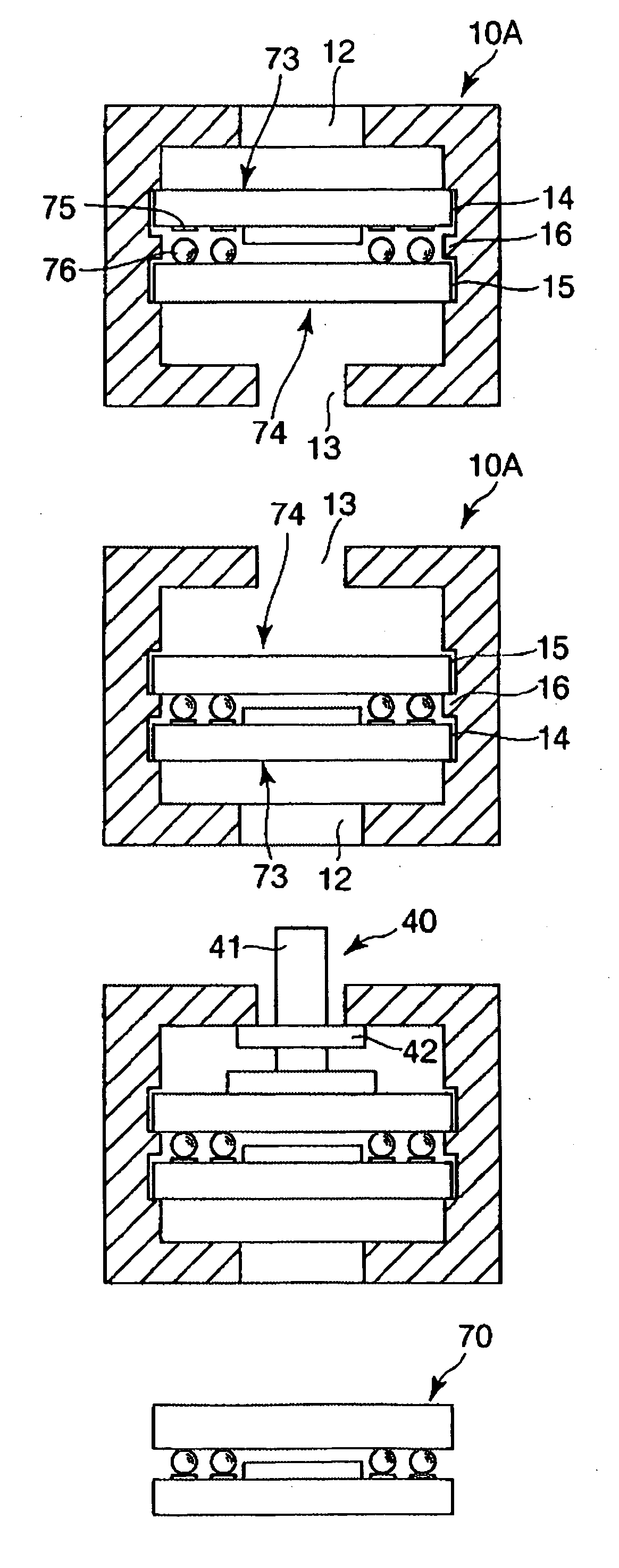
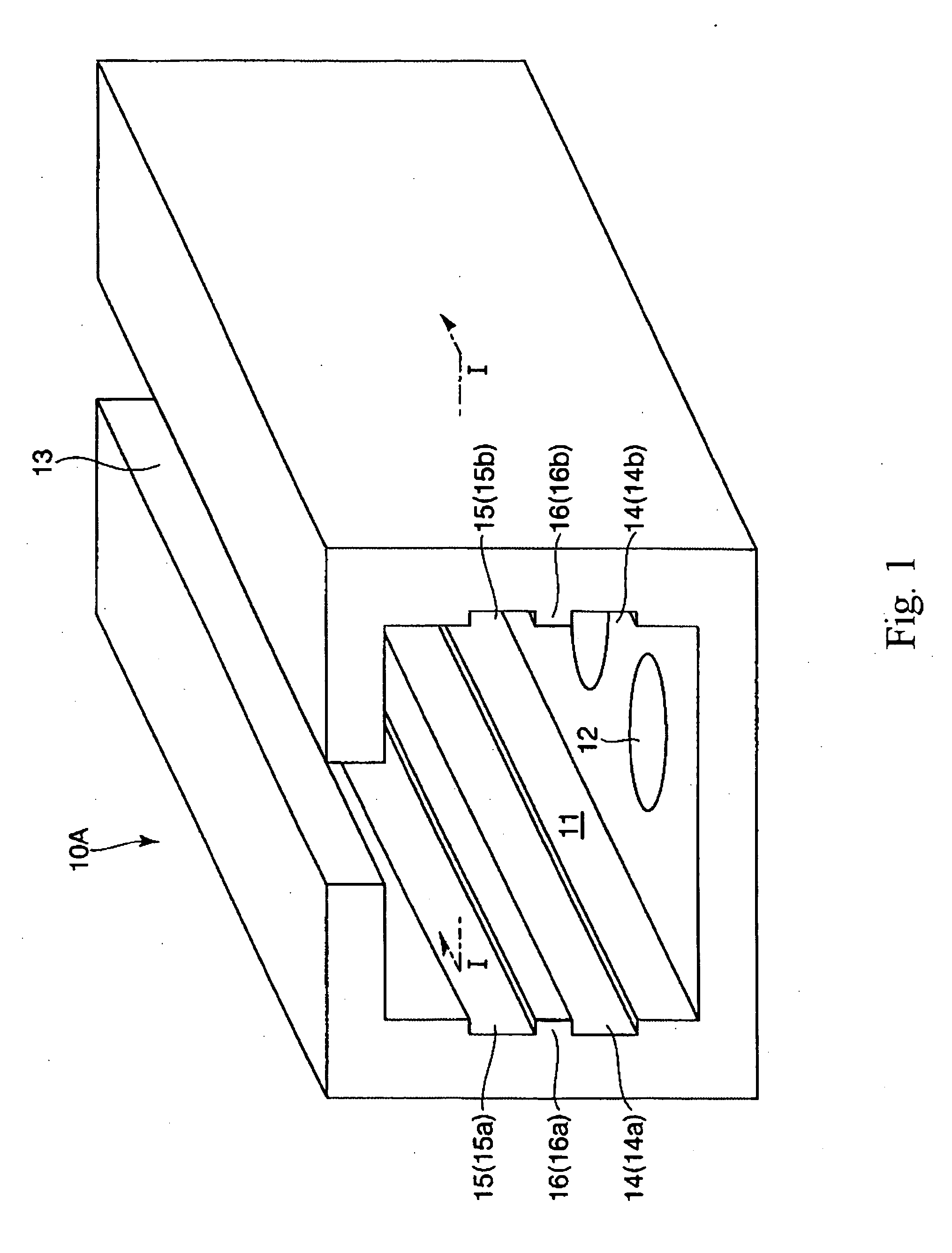
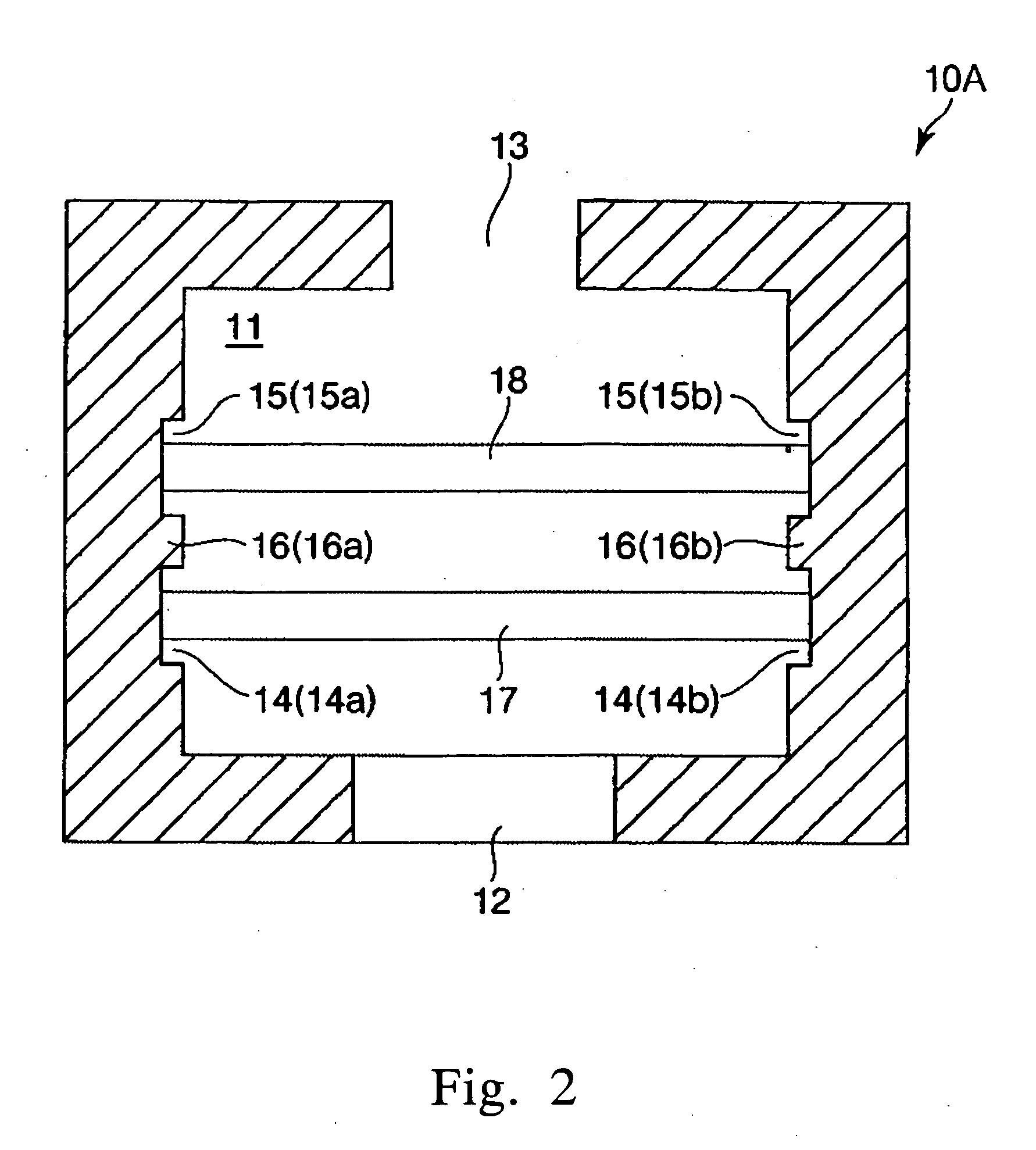
[0059]FIG. 1 is a perspective view which shows an apparatus for manufacturing semiconductor devices according to the first embodiment of the present invention, FIG. 2 is a cross-sectional view taken along the lines I-I in FIG. 1, and FIG. 3 is a drawing which shows one example structure of a substrate for mounting semiconductor components (lower semiconductor package), wherein FIG. 3(a) is a cross-sectional view of the substrate for mounting semiconductor components, and FIG. 3(b) is a plan view of the substrate for mounting semiconductor components. Further, FIG. 4 is a drawing which shows one example structure of semiconductor components (upper semiconductor package), wherein FIG. 4(a) is a cross-sectional view of the semiconductor components, and FIG. 4(b) is a plan view of the semiconductor components. Further, FIG. 5 is a cross-secti...

second embodiment

[0103]FIG. 8 is a perspective view which shows an apparatus for manufacturing semiconductor devices according to the present invention, FIG. 9 and FIG. 10 are drawings which shows one example of a method of manufacturing semiconductor devices using the apparatus for manufacturing semiconductor devices shown in FIG. 8. Further, in the description given below, the upper side in FIG. 8 to FIG. 10 is referred to as “upper”, and the lower side is referred to as “lower”.

[0104] First, the structure of an apparatus 10B for manufacturing semiconductor devices of the second embodiment will be described.

[0105] As shown in FIG. 8, in addition to the first guide grooves 14a, 14b, the second guide grooves 15a, 15b, and the protruding portions 16a, 16b arranged in the longitudinal direction described above on both sides facing the insertion space 11, the apparatus 10B for manufacturing semiconductor devices further includes partition grooves 51a, 51b formed inside the second guide grooves 15a, 15...

third embodiment

[0114]FIG. 11 is a perspective view which shows an apparatus for manufacturing semiconductor devices according to the present invention, FIG. 12 is a cross-sectional view taken along the lines II-II in FIG. 11, FIG. 13 is a cross-sectional view which shows one process in a manufacturing method using the apparatus for manufacturing semiconductor devices shown in FIG. 11 and FIG. 12, and FIG. 14 is a cross-sectional view which shows one example structure of a semiconductor device manufactured by the apparatus for manufacturing semiconductor devices shown in FIG. 11 and FIG. 12. Further, the upper side in FIG. 11 and FIG. 13 is referred to as “upper”, and the lower side is referred to as “lower”.

[0115] As shown in FIG. 11 and FIG. 12, an apparatus 10C for manufacturing semiconductor devices of the third embodiment is provided with two sets of the second guide grooves 15a, 15b which loosely hold upper semiconductor packages 74′ (which are movably supported in the first direction), respe...


PUM

PropertyMeasurementUnit
thicknessaaaaaaaaaa
thicknessaaaaaaaaaa
thicknessaaaaaaaaaa

Abstract

An apparatus for manufacturing semiconductor devices having a roughly rectangular parallelepiped box-shape includes an internal insertion space for semiconductor packages, first guide grooves and arranged along the longitudinal direction in both side surfaces facing the insertion space and second guide grooves and arranged parallel to the first guide grooves and respectively. Edge portions of an upper semiconductor package (a semiconductor component) are loosely fitted into the second guide grooves so that the movement of the upper semiconductor package in the left and right direction is restricted. Further, edge portions of a lower semiconductor package (a substrate for mounting semiconductor components) are loosely fitted into the first guide grooves so that the movement of the lower semiconductor package in the left and right direction is restricted. By using the apparatus, it becomes possible to provide a semiconductor device in which poor connections are difficult to occur, and further to provide an apparatus for manufacturing semiconductor devices and a method of manufacturing semiconductor devices that enable to prevent the occurrence of such poor connections in the obtained semiconductor devices and also enable to reduce manufacturing costs.

Description

BACKGROUND OF THE INVENTION [0001] 1. Field of the Invention [0002] The present invention relates to an apparatus for manufacturing semiconductor devices, a method of manufacturing the semiconductor devices, and a semiconductor device manufactured by the apparatus and method. [0003] 2. Description of the Prior Art [0004] In general, when manufacturing a semiconductor device, a semiconductor chip is mounted on top of a substrate, and then a process for connecting the semiconductor chip and the substrate is carried out by soldering. [0005] In the prior art, this kind of process is carried out by a method like that disclosed in Japanese Laid-Open Patent Application No. H 11-97839 (see lines 14 to 24 in the left column of page 10), for example. [0006] Namely, using a mounter, a semiconductor chip (semiconductor component) is mounted on top of a substrate (that is, a substrate for mounting semiconductor components), and then the substrate having the semiconductor chip mounted thereon is ...

Claims


Application Information

Patent Timeline
Patent Type & Authority Applications(United States)
IPC IPC(8): B23P19/00H01L21/00H01L21/60H01L25/10H01L25/11H01L25/18H05K1/18H01L27/095H01L29/47H01L29/812H01L31/07H01L31/108
CPCH01L25/50H01L2224/16Y10T29/53183Y10T29/53178Y10T29/53174
Inventor NISHIYAMA, YOSHIHIDE
Owner SEIKO EPSON CORP
Why Eureka
Try Eureka