Semiconductor memory device

Inactive Publication Date: 2005-04-07
JAPAN ENG +1
View PDF4 Cites 8 Cited by
  • Summary
  • Abstract
  • Description
  • Claims
  • Application Information

AI Technical Summary

Benefits of technology

[0003] In the related art 1, no page read mode is disclosed. The related art 1 does not show architecture for performing switching to a high-speed sequential read mode when only a column address has changed. The related art 2 has a problem in that it co

Problems solved by technology

The related art 2 has a problem in that it corresponds to a page read mode but pays no consideration to the refresh operation, and when page read is

Method used


Image

  • Semiconductor memory device
  • Semiconductor memory device
  • Semiconductor memory device

Examples


Embodiment Construction

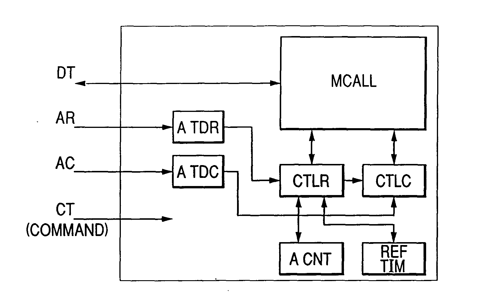
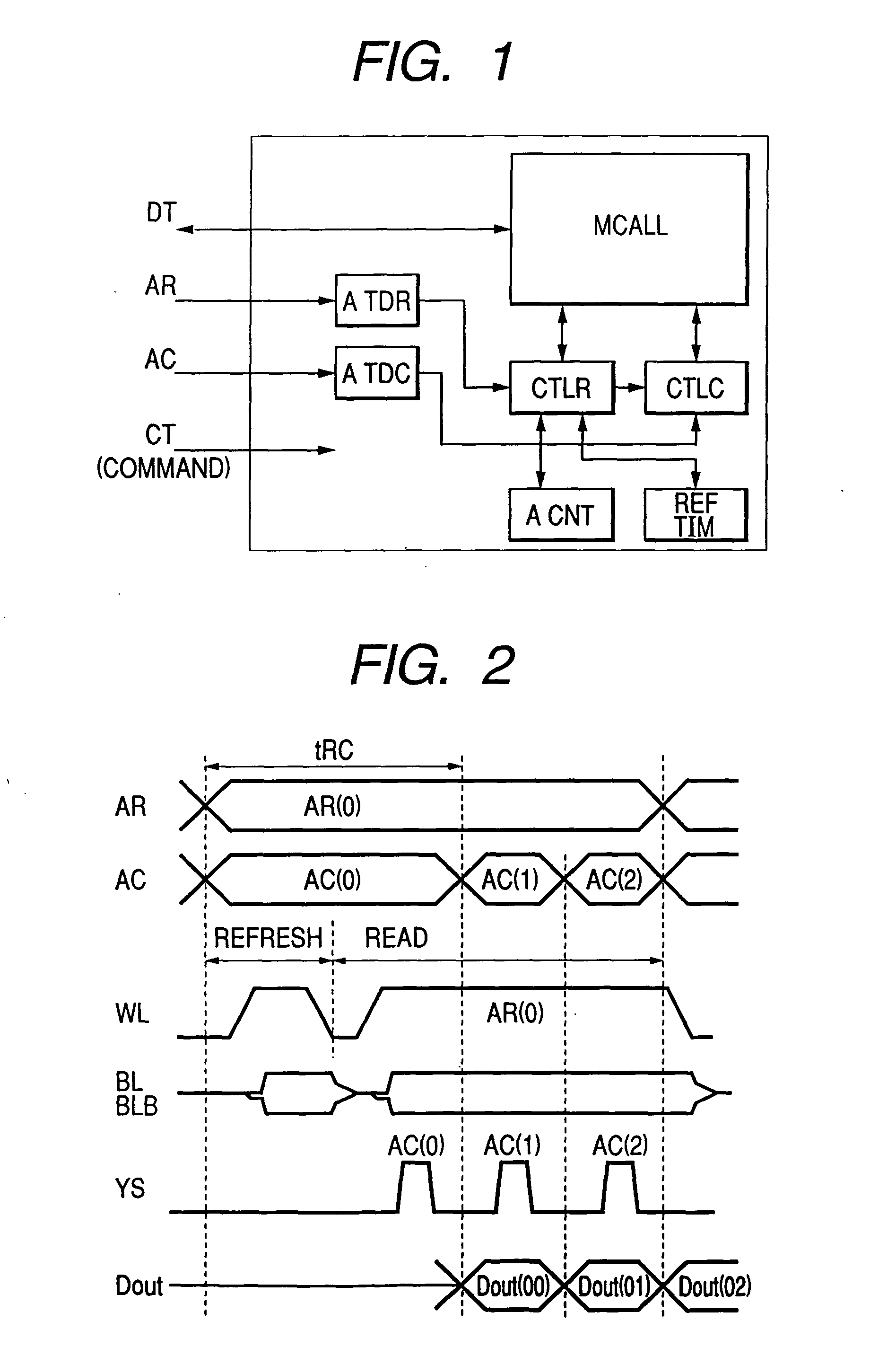
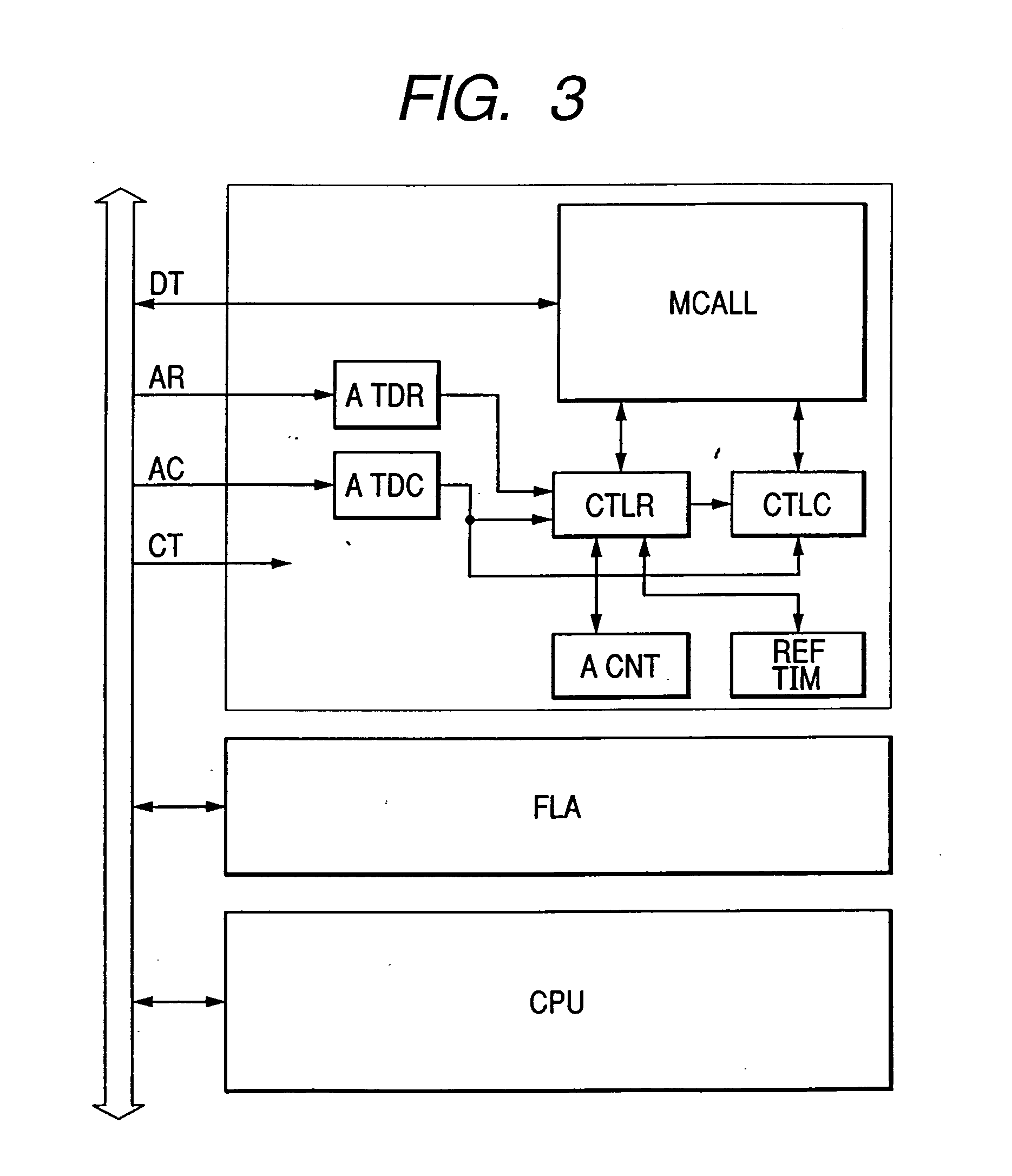
[0038] A schematic block diagram showing one embodiment of a semiconductor memory device according to the present invention is shown in FIG. 1. In the semiconductor memory device showing the present embodiment, a memory circuit MCALL includes a plurality of memory cells which are provided so as to correspond to a plurality of bit lines and a plurality of word lines and each of which needs a refresh operation for periodically holding memory information therein. Each of the memories comprises, for example, an information storage capacitor and an address selection MOSFET. The gate of the address selection MOSFET is electrically connected to its corresponding word line, one of its source and drain paths is electrically connected to its corresponding bit line. the other thereof is electrically connected to its corresponding storage node of the storage capacitor.

[0039] The bit lines are provided in pairs and connected to an input / output node of a sense amplifier comprising differential l...


PUM


Abstract

With the objective of providing a semiconductor memory device which is made identical in usability to a static RAM by use of dynamic memory cells and realizes a high-speed memory cycle time, there is provided a pseudo static RAM having a time multiplex mode which, when instructions for a memory operation for reading memory information from each of memory cells each requiring a refresh operation for periodically holding the memory information, or writing the same therein is issued, carries out an addressing-based autonomous refresh operation different from the memory operation before or after the memory operation. The pseudo static RAM includes address signal transition detectors for a row and a column, and a page mode which independently performs a column address selecting operation according to an address signal transition detect signal of the second address signal transition detector.

Description

BACKGROUND OF THE INVENTION [0001] The present invention relates to a semiconductor memory device which needs a refresh operation, and principally to a technology effective for application to a pseudo static RAM or the like which executes an external read / write operation and a refresh operation executed by an internal circuit during one memory cycle to conceal the refresh operation from outside, thereby being usable equivalently to a static RAM (Random Access Memory) on an equivalent basis. [0002] In order to make it possible to handle a DRAM in a manner similar to an SRAM (Static Random Access Memory), a so-called time multiplex type DRAM wherein a read / write operation and a refresh operation are executed during one cycle with their times being assigned thereto, or the two operations are executed only when the read / write operation and the refresh operation compete with each other, has been proposed in Unexamined Patent Publication No. Sho 61(1985)-71494 (Related Art 1). Further, a ...

Claims


Application Information

Patent Timeline
IPC IPC(8): G11C11/403G11C7/00G11C11/34G11C11/401G11C11/406
CPCG11C11/406G11C2211/4061G11C11/408G11C11/40615G11C11/34
Inventor YAHATA, HIDEHARUHORIGUCHI, MASASHISAITOH, YOSHIKAZUKAWASE, YASUSHI
Owner JAPAN ENG
Why Eureka
Try Eureka