GaN/AIGaN/GaN dispersion-free high electron mobility transistors

a high electron mobility, transistor technology, applied in the direction of semiconductor devices, electrical equipment, basic electric elements, etc., can solve the problems of poor reproducibility and achieve the effect of high electron mobility

Inactive Publication Date: 2005-04-14
RGT UNIV OF CALIFORNIA
View PDF5 Cites 120 Cited by
  • Summary
  • Abstract
  • Description
  • Claims
  • Application Information

AI Technical Summary

Benefits of technology

[0008] To overcome the limitations in the prior art described above, and to overcome other limitations that will become apparent upon reading and understanding the present specification, the present invention discloses a dispersion-free high electron mobility transistor (HEMT), comprised of a substrate; a semi-insulating buffer layer, comprised of gallium nitride (GaN) or aluminum gallium nitride (AlGaN), deposited on the substrate, an AlGaN barrier layer, with an aluminum (Al) mo...

Problems solved by technology

This dispersion has been reported to be due to the slow response of the surface traps.
In the prior art, silicon nitride (SiN) passivation has been used to sup...

Method used


Image

  • GaN/AIGaN/GaN dispersion-free high electron mobility transistors
  • GaN/AIGaN/GaN dispersion-free high electron mobility transistors
  • GaN/AIGaN/GaN dispersion-free high electron mobility transistors

Examples


Embodiment Construction

[0018] In the following description of the preferred embodiment, reference is made to the accompanying drawings which form a part hereof, and in which is shown by way of illustration a specific embodiment in which the invention may be practiced. It is to be understood that other embodiments may be utilized and structural changes may be made without departing from the scope of the present invention.

[0019] General Description

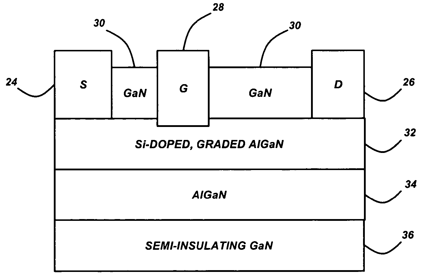
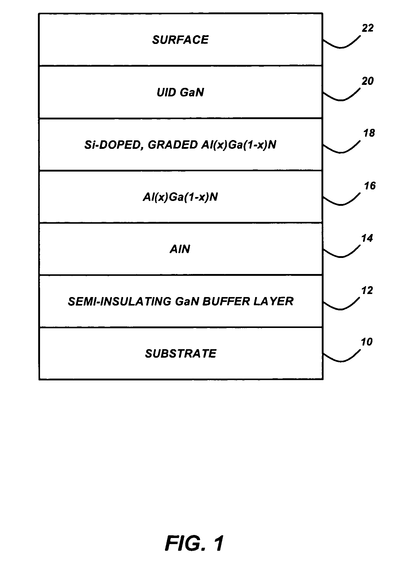
[0020] The present invention uses an epitaxial solution to suppress the “DC-to-RF” dispersion problem suffered by GaN power HEMTs. This epitaxial solution results in the novel epitaxial structure of a GaN / AlGaN / GaN HEMT shown in FIG. 1, comprising a sapphire or silicon carbide (SiC) substrate 10, semi-insulating (S.I.) GaN buffer layer 12, AlN layer 14, AlxGa1-xN layer 16, silicon-doped (Si-doped), graded AlxGa1-xN layer 18, GaN cap 20 and surface 22.

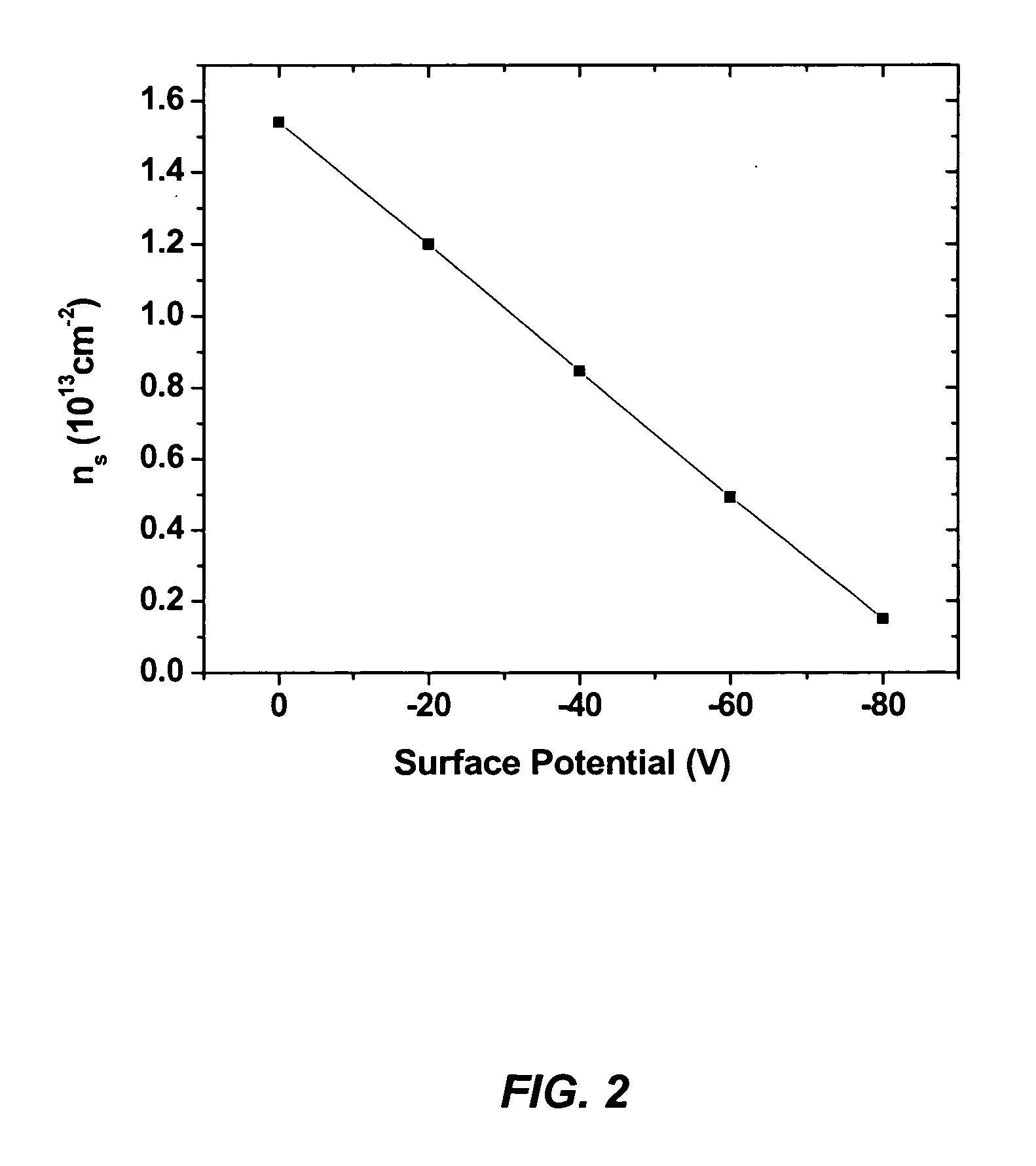
[0021] In this structure, the GaN cap 20 is unintentionally doped (UID). The amount of dispersion depends on a r...


PUM


Abstract

A dispersion-free high electron mobility transistor (HEMT), comprised of a substrate; a semi-insulating buffer layer, comprised of gallium nitride (GaN) or aluminum gallium nitride (AlGaN), deposited on the substrate, an AlGaN barrier layer, with an aluminum (Al) mole fraction larger than that of the semi-insulating buffer layer, deposited on the semi-insulating buffer layer, an n-type doped graded AlGaN layer deposited on the AlGaN barrier layer, wherein an Al mole fraction is decreased from a bottom of the n-type doped graded AlGaN layer to a top of the n-type doped graded AlGaN layer, and a cap layer, comprised of GaN or AlGaN with an Al mole fraction smaller than that of the AlGaN barrier layer, deposited on the n-type doped graded AlGaN layer.

Description

CROSS-REFERENCE TO RELATED APPLICATIONS [0001] This application claims the benefit under 35 U.S.C. §119(e) of the following co-pending and commonly-assigned U.S. Provisional Patent Application Ser. No. 60 / 510,695, entitled “GaN / AlGaN / GaN dispersion-free high electron mobility transistors,” filed on Oct. 10, 2003, by Likun Shen, Sten J. Heikman and Umesh K. Mishra, attorneys docket number 30794.107-US-P1; which application is incorporated by reference herein.STATEMENT REGARDING FEDERALLY SPONSORED RESEARCH AND DEVELOPMENT [0002] This invention was made with Government support under Grant No. N00014-01-1-0764 awarded by the CANE MURI program. The Government has certain rights in this invention.BACKGROUND OF THE INVENTION [0003] 1. Field of the Invention [0004] This invention relates to semiconductor devices, and more particularly, to gallium nitride / aluminum gallium nitride / gallium nitride (GaN / AlGaN / GaN) dispersion-free high electron mobility transistors (HEMTs). [0005] 2. Descriptio...

Claims


Application Information

Patent Timeline
IPC IPC(8): H01L21/335H01L29/20H01L29/778
CPCH01L29/2003H01L29/7787H01L29/66462
Inventor SHEN, LIKUNHEIKMAN, STEN JOHANMISHRA, UMESH KUMAR
Owner RGT UNIV OF CALIFORNIA
Why Eureka
Try Eureka