Semiconductor device having periodic construction

Inactive Publication Date: 2005-04-14
DENSO CORP
View PDF15 Cites 27 Cited by
  • Summary
  • Abstract
  • Description
  • Claims
  • Application Information

AI Technical Summary

Benefits of technology

[0007] In view of the above-described problem, it is an object of the present invention to

Problems solved by technology

Thus, the device has a high withstand

Method used


Image

  • Semiconductor device having periodic construction
  • Semiconductor device having periodic construction
  • Semiconductor device having periodic construction

Examples


first embodiment

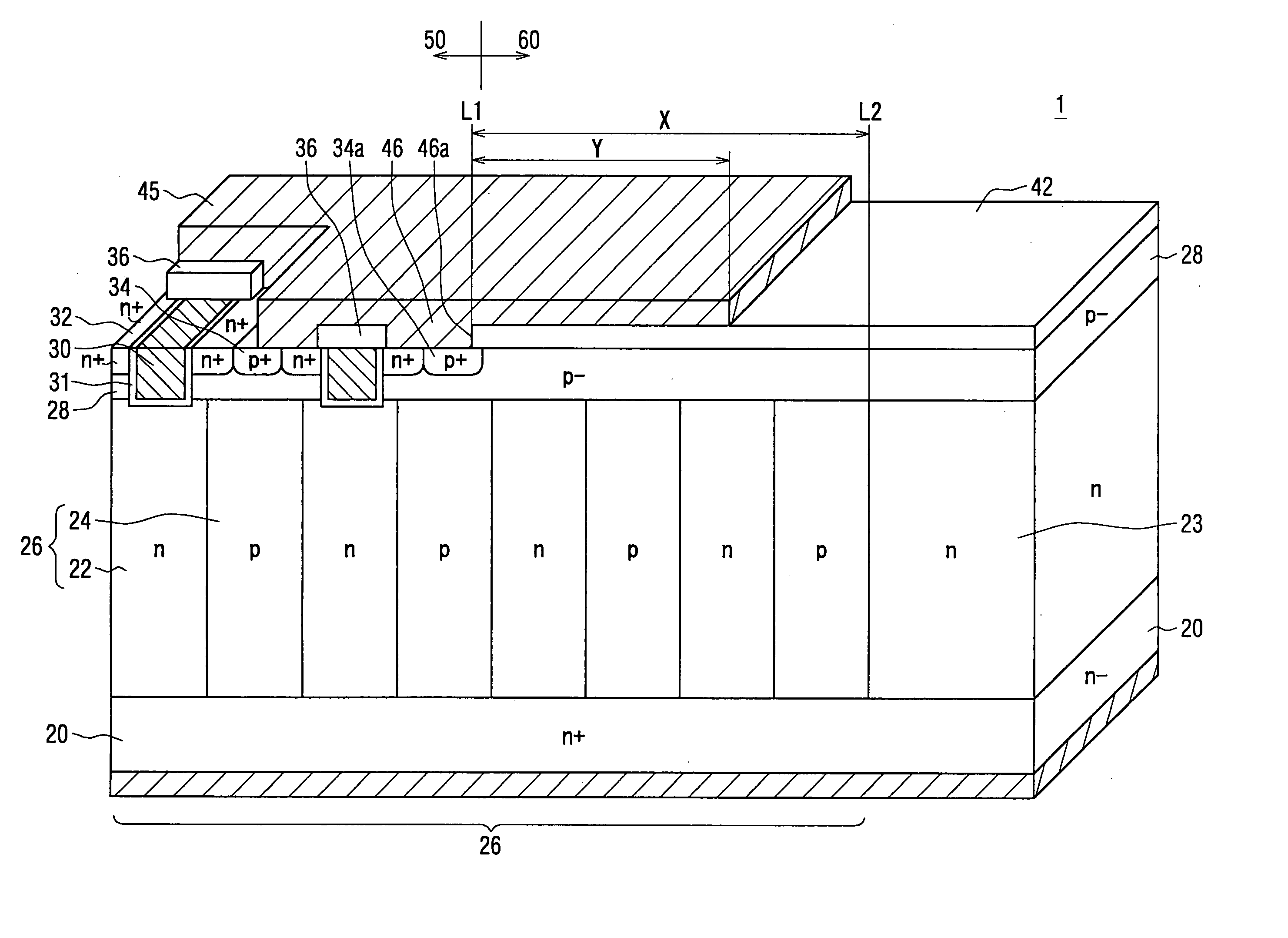
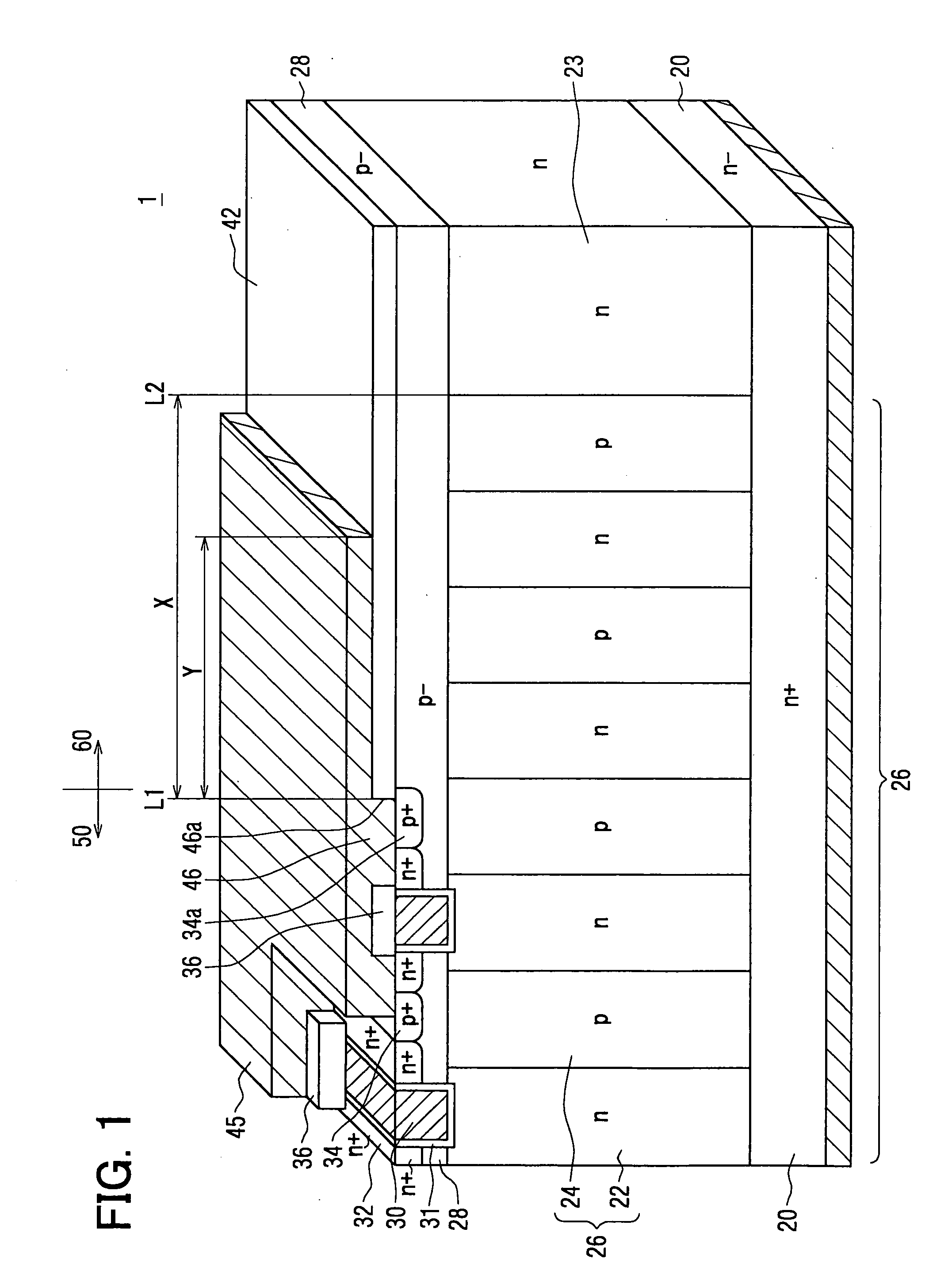
[0026] The inventors have preliminarily studied about a semiconductor device having a super junction construction. Specifically, the device includes a periphery portion and a center portion. Both of the center portion and the periphery portion have the super junction construction. The super junction construction includes a P type column and an N type column, which provide a periodic construction and are alternately disposed and repeated in a repeating direction. By using a P type contact region disposed in the center portion, the P type column disposed in the periphery portion is connected to a source electrode. A brake down phenomenon occurred in the periphery portion is studied by the inventors. As a result, electric field is concentrated at around an interface between a contact region disposed on utmost outer periphery of the center portion and a part of the periphery portion, which has the same conductive type as the contact region. Thus, the brake down phenomenon is occurred ar...

second embodiment

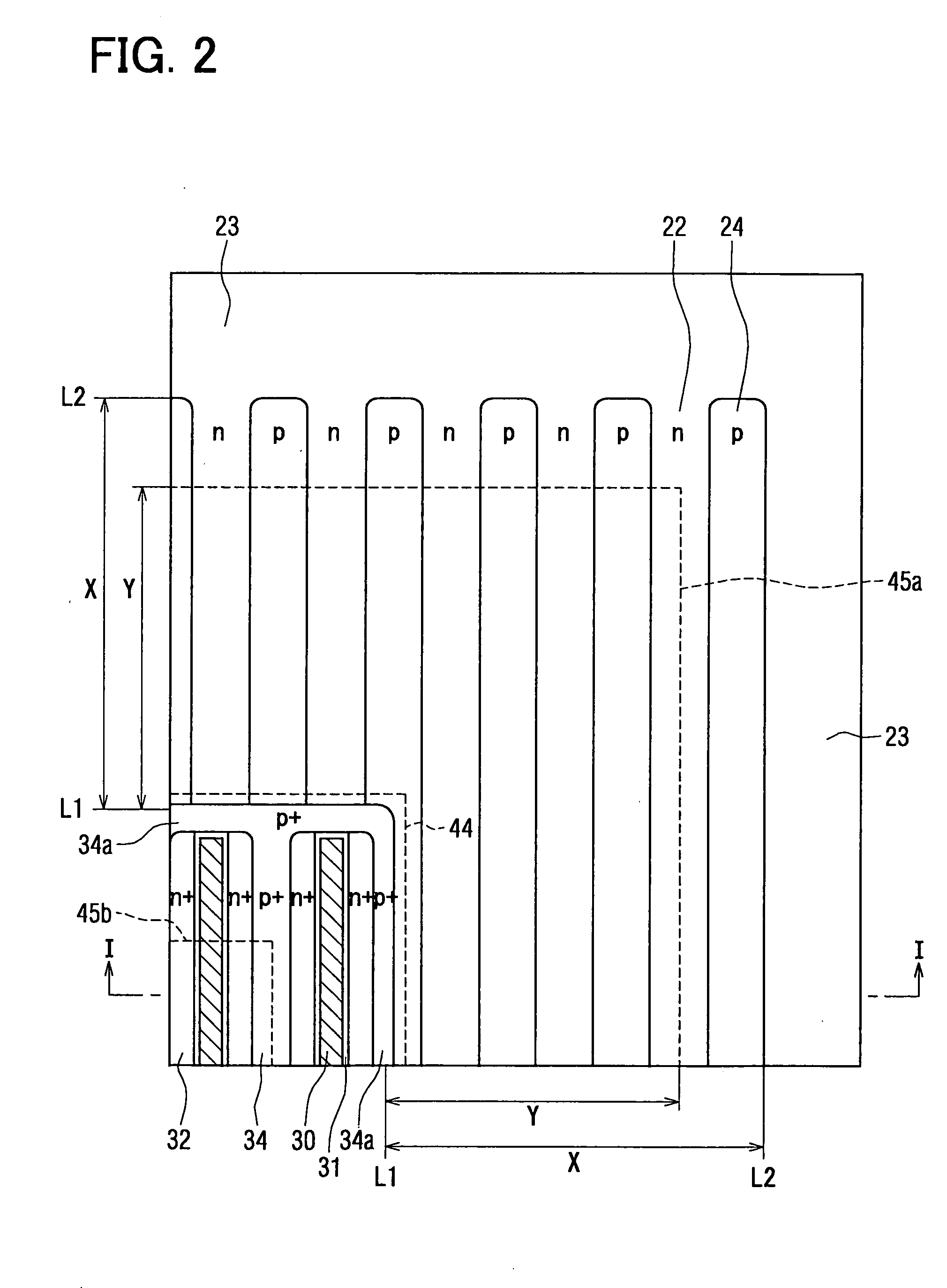
[0053] A semiconductor device 2 according to a second embodiment of the present invention is shown in FIG. 3. FIG. 3 is a partial cross sectional view showing the device 1 in FIG. 1. FIG. 3 shows an equipotential line distribution of a brake down voltage. Each broken line shows an equipotential line so that the brake down voltage on the same broken line is constant. The brake down voltage is determined in a case where a positive voltage is applied to the first semiconductor layer 20 and the potential of the source electrode 45 is set to be zero. In the device 2, a charge valance between the N type column 22 as the first region and the P type column 24 as the second region is held appropriately. The extension length Y of the source electrode 45 is three-fourths of the distance X between the line L1 and the end line L2. Five units composed of the N type column 22 and the P type column 24 are disposed between the line L1 and the end line L2.

[0054] Another semiconductor device 3 as a c...

third embodiment

[0061] A semiconductor devices 7, 10 according to a third embodiment of the present invention have different numbers of the units composed of the N type column 22 and the P type column 24. Specifically, the device 7 has seven units, and the device 10 has ten units, although the device 2 has five units. FIG. 9 shows a relationship between the withstand voltage and the ratio of the extension length Y and the distance X. Curve 7 represents the device 7, and curve 10 represents the device 10.

[0062] As shown in FIGS. 8 and 10, the withstand voltage of each device 2, 7, 10 is increased without depending on the number of the units of the periodic construction 26 substantially. Therefore, the ratio of the extension length Y and the distance X mainly affects the increase of the withstand voltage of the device 2, 7, 10. Further, when the electrode 45 extends to the interface between the periodic construction 26 and the end region 23, i.e., when the ratio of the extension length Y is one, the...


PUM


Abstract

A device includes a center portion, and a periphery portion disposed around the center portion. The periphery portion includes a first semiconductor layer, an intermediate layer, a second semiconductor layer, an insulation layer and an electrode. The intermediate layer includes a periodic construction having a first region and a second region. The center portion includes a contact region. The electrode extends to the periphery portion to have an extension length of the electrode between the contact region and a periphery of the electrode. The extension length of the electrode is equal to or longer than one-eighth of a distance between the contact region and an outer periphery of the periodic construction.

Description

CROSS REFERENCE TO RELATED APPLICATION [0001] This application is based on Japanese Patent Application No. 2003-352335 filed on Oct. 10, 2003, the disclosure of which is incorporated herein by reference. FIELD OF THE INVENTION [0002] The present invention relates to a semiconductor device having a periodic construction. BACKGROUND OF THE INVENTION [0003] A semiconductor device having a periodic construction, i.e., a super junction construction is disclosed in Unexamined Japanese Patent Application Publication No. 2002-184985 (which corresponds to U.S. Pat. No. 6,639,260-B2 and U.S. patent application Publication No. 2002-0074596-A1). The super junction construction is such that the device includes the first region having the first conductive type and the second region having the second conductive type, which are laminated each other in a horizontal direction (i.e., a repeating direction). Specifically, the first conductive type is a N type conductivity, and the second conductive typ...

Claims


Application Information

Patent Timeline
IPC IPC(8): H01L29/06H01L29/40H01L29/417H01L29/78
CPCH01L29/0619H01L29/0634H01L29/7813H01L29/402H01L29/41741H01L29/0696H01L29/7811
Inventor YAMAUCHI, SHOICHISUZUKI, MIKIMASAHATTORI, YOSHIYUKINAKASHIMA, KYOKO
Owner DENSO CORP
Why Eureka
Try Eureka