Integrated circuit package

a technology of integrated circuits and circuit components, applied in the direction of semiconductor devices, semiconductor/solid-state device details, electrical equipment, etc., can solve the problem that the semiconductor device generates a great deal of heat during normal operation

Inactive Publication Date: 2005-04-14
ASAT CO LTD
View PDF99 Cites 74 Cited by
  • Summary
  • Abstract
  • Description
  • Claims
  • Application Information

AI Technical Summary

Problems solved by technology

A semiconductor device generates a great deal of heat during normal operation.

Method used


Image

  • Integrated circuit package
  • Integrated circuit package
  • Integrated circuit package

Examples


Embodiment Construction

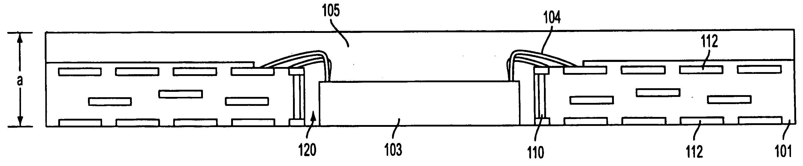
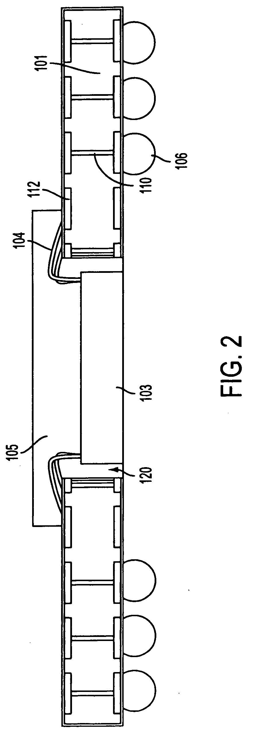
[0014] Various embodiments of the integrated circuit package and various examples of methods for manufacturing integrated circuit packages according to the present invention will now be described with reference to the drawings.

[0015]FIGS. 1 and 2 show certain components of integrated circuit packages according to embodiments of the present invention. The integrated circuit packages depicted in FIGS. 1 and 2 each generally include a substrate 101, a semiconductor die 103 and an encapsulant 105. The substrate 101 may be made of either a rigid material (e.g., BT, FR4, FR5 or ceramic) or a flexible material (e.g., polyimide), and may have circuit traces 112 onto which a semiconductor die 103 may be interconnected using, for example, wire bonding techniques or tape automated bonding. In the embodiment shown in FIG. 1, the package measures about 1.0 mm thick (shown as dimension “a” in FIG. 1) and about 35 mm wide (shown as dimension “b” in FIG. 3). The width dimension of certain other em...


PUM

PropertyMeasurementUnit
thickaaaaaaaaaa
thickaaaaaaaaaa
widthaaaaaaaaaa

Abstract

In one aspect, the present invention features a method of manufacturing an integrated circuit package including providing a substrate having a first surface, a second surface opposite the first surface, a cavity through the substrate between the first and second surfaces and a conductive via extending through the substrate and electrically connecting the first surface of the substrate with the second surface of the substrate, applying a strip to the second surface of the substrate, mounting a semiconductor die on the strip, at least a portion of the semiconductor die being disposed inside the cavity, encapsulating in a molding material at least a portion of the first surface of the substrate, and removing the strip from the substrate. In another aspect, the invention features an integrated circuit package including a substrate having a first surface, a second surface opposite the first surface, a cavity through the substrate between the first and second surfaces and a conductive via extending through the substrate and electrically connecting the first surface of the substrate with the second surface of the substrate, a semiconductor die electrically coupled with the conductive via, at least a portion of the semiconductor die being disposed inside the cavity of the substrate, an encapsulant material encapsulating a portion of the semiconductor die such that at least a portion of a surface of the semiconductor die is exposed.

Description

FIELD OF THE INVENTION [0001] The present invention relates to integrated circuit packaging and manufacturing thereof, and more particularly, to integrated circuit packaging for improved dissipation of thermal energy. BACKGROUND OF THE INVENTION [0002] A semiconductor device generates a great deal of heat during normal operation. As the speed of semiconductors has increased, so too has the amount of heat generated by them. It is desirable to dissipate this heat from an integrated circuit package in an efficient manner. [0003] A heat sink is one type of device used to help dissipate heat from some integrated circuit packages. Various shapes and sizes of heat sink devices have been incorporated onto, into or around integrated circuit packages for improving heat dissipation from the particular integrated circuit package. For example, U.S. Pat. No. 5,596,231 to Combs, entitled “High Power Dissipation Plastic Encapsulated Package For Integrated Circuit Die,” discloses a selectively coate...

Claims


Application Information

Patent Timeline
Patent Type & Authority Applications(United States)
IPC IPC(8): H01L21/56H01L21/68H01L23/13H01L23/538H01L25/10
CPCH01L21/566H01L21/568H01L23/13H01L23/5389H01L24/97H01L25/105H01L2224/48091H01L2224/48227H01L2224/85001H01L2224/97H01L2924/01029H01L2924/01047H01L2924/01079H01L2924/01082H01L2924/14H01L2924/15311H01L2924/18165H01L24/48H01L2924/01005H01L2924/01006H01L2924/01033H01L2225/1035H01L2225/1058H01L2225/1094H01L2224/45144H01L2224/32245H01L2224/73265H01L24/45H01L24/73H01L2924/181H01L2224/85H01L2924/00014H01L2924/00012
Inventor MCLELLAN, NEILFAN, CHUNCOMBS, EDWARDCHEUNG, TSANGKEUNG, CHOWLABEEB, SADAK
Owner ASAT CO LTD
Why Eureka
Try Eureka