Method for producing a multichip module and multichip module

Inactive Publication Date: 2005-04-14
POLARIS INNOVATIONS
View PDF19 Cites 23 Cited by
  • Summary
  • Abstract
  • Description
  • Claims
  • Application Information

AI Technical Summary

Benefits of technology

[0013] In another embodiment of the invention, a multiplicity of chips in a chip stack can advantageously be connected to one another in a simple and cost-effective manner. The use of cost-intensive rewiring substrates or disadvantageous bonding wires can thus be avoided. Following the production method according to the invention, a high

Problems solved by technology

What is problematic in the case of SiP solutions is that the individual chips within the package, preferably within a chip stack, have to be electrically conductively connected together among one another.
Based on the high inductance and capacitance of the bonding wire, many connecting points and a lack of impedance matching.
Such an arrangement gives rise to long signal paths, however, which likewise result in poor electrical prop

Method used


Image

  • Method for producing a multichip module and multichip module
  • Method for producing a multichip module and multichip module
  • Method for producing a multichip module and multichip module

Examples


Example

[0037] In the figures, identical reference symbols designate identical or functionally identical component parts.

DETAILED DESCRIPTION OF THE INVENTION

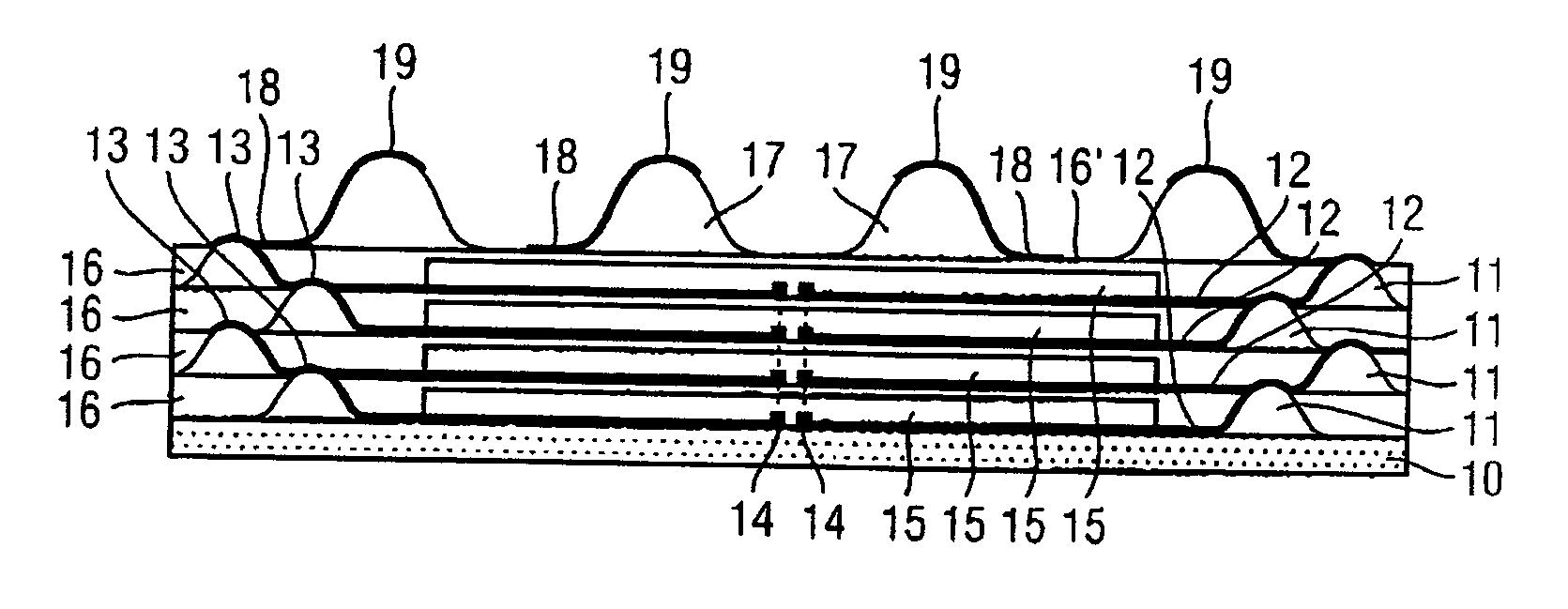
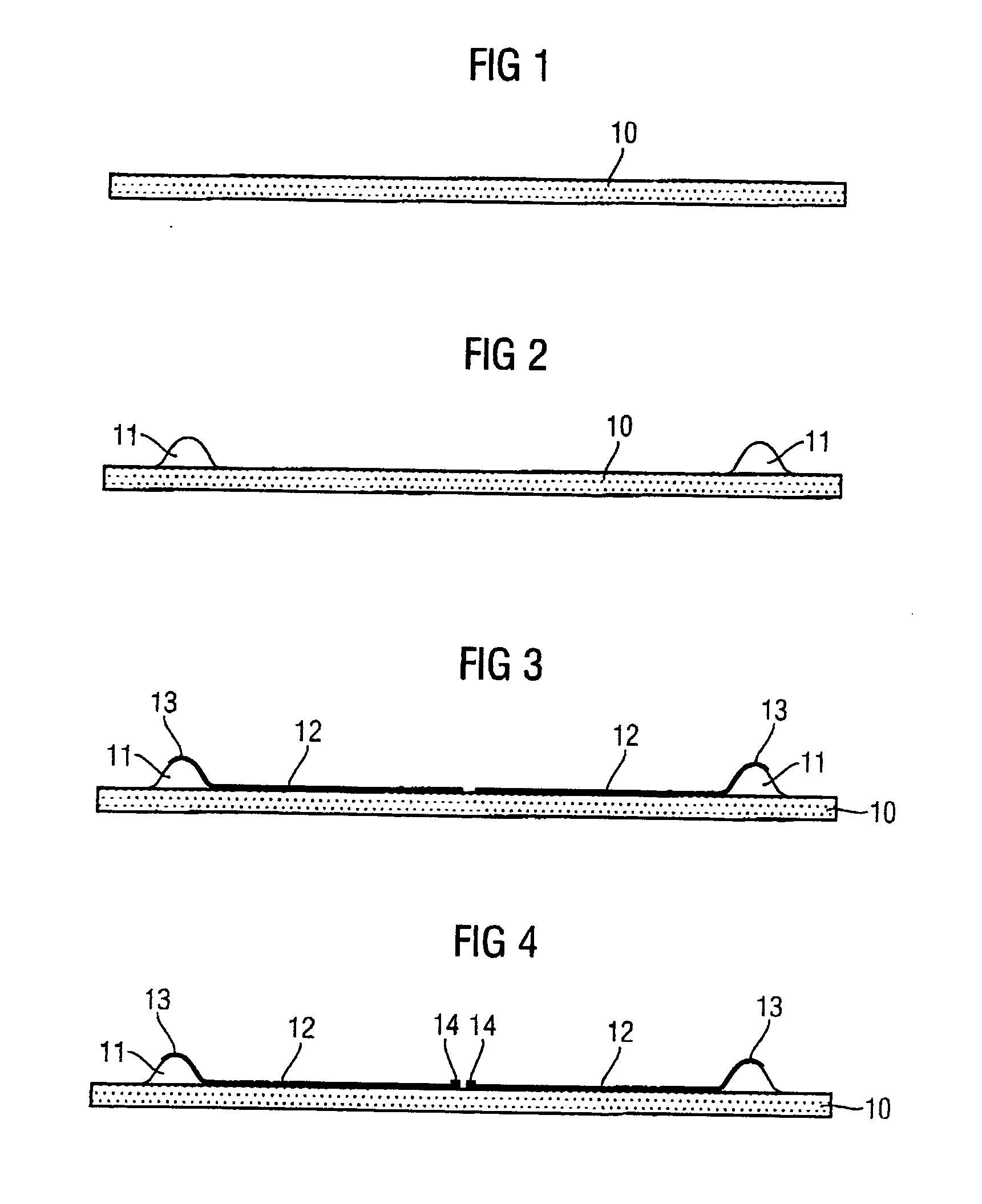
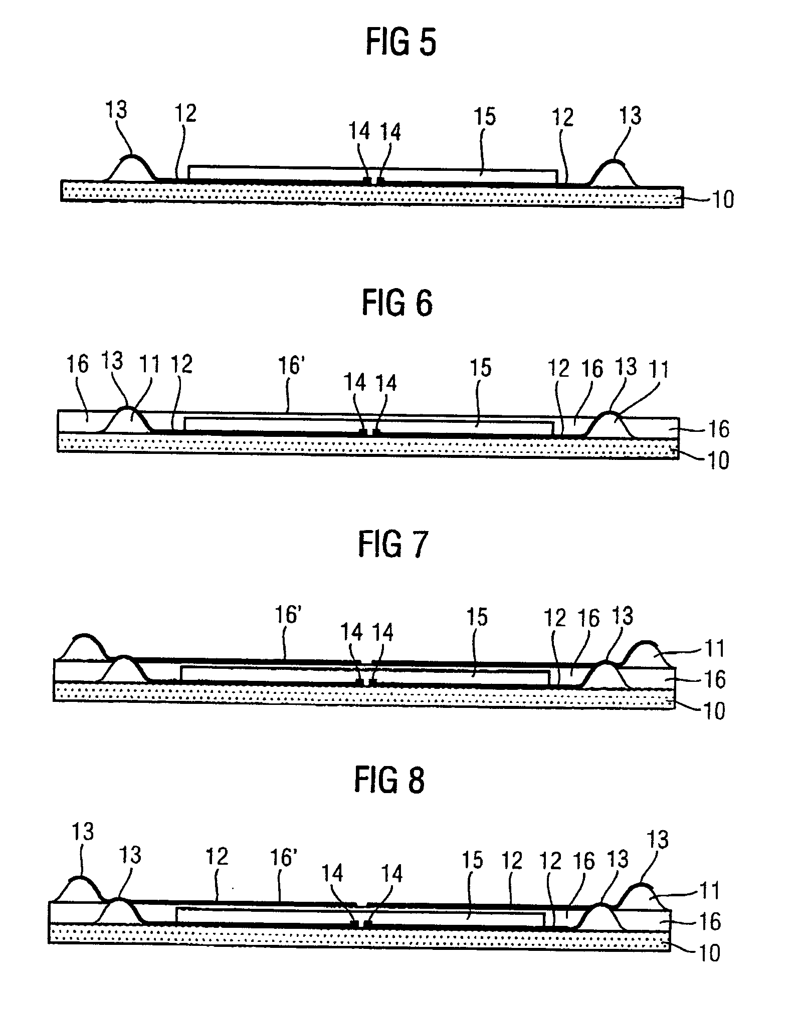
[0038]FIG. 1 illustrates a substrate 10, preferably a sheet, in cross section. In accordance with FIG. 2, at least one contact elevation 11 is applied thereto. The contact elevation 11 is made of a polymer, for example, which may be conductive, such as conductive adhesive, for example, or nonconductive, such as silicone, polyurethane, polyimide, for example. The application of the at least one contact elevation 11 is preferably effected in a printing operation or a metering operation or an injection-molding operation or a stamping step. The at least one contact elevation 11 is preferably bell-shaped and has a small gradient in the transition from the substrate 10 to the contact elevation 11. In this connection, a small gradient is understood to be a gradient of less than 0.5.

[0039] In accordance with FIG. 3, a rewiring device 12 is ...


PUM


Abstract

A method for producing a multi-chip module having application of at least one contact elevation onto a substrate, application and patterning of a rewiring device onto the substrate and the at least one contact elevation with provision of a contact device on the at least one contact elevation, application of a semiconductor chip onto the substrate with electrical contact-connection of the rewiring device; application of an encapsulating device that is not electrically conductive onto the semiconductor chip, the substrate, the rewiring device and the at least one contact elevation, the contact device on the at least one contact elevation at least touching a first surface of the encapsulating device; and repetition at least once of at least the first two steps, the first surface of the encapsulating device serving as a substrate and the correspondingly produced rewiring device making electrical contact with the contact device of the at least one contact elevation of the underlying plane.

Description

CLAIM FOR PRIORITY [0001] This application claims the benefit of priority to German Application No. 103 45 391.1, which was filed in the German language on Sep. 30, 2003, the contents of which are hereby incorporated by reference. [0002] 1. Technical Field of the Invention [0003] The present invention relates to a method for producing a multichip module and a corresponding multichip module, and in particular, to a method for producing a multichip system in a package. [0004] 2. Background of the Invention [0005] In order to be able to provide complete semiconductor system solutions, it is necessary to be able to integrate different functional units within a component. For such integration, it is possible on the one hand to choose an SoC approach (system on chip) or on the other hand an SiP approach (system in a package). SiP solutions afford the advantage that, within a package, separate chips can in each case be individually optimized, tested and produced cost-effectively as functio...

Claims


Application Information

Patent Timeline
IPC IPC(8): H01L21/60H01L21/98H01L25/18H01L23/538H01L25/065H01L25/07
CPCH01L23/5389H01L24/18H01L2924/12041H01L2224/32225H01L2224/32145H01L2924/014H01L2924/01033H01L2924/01006H01L2924/01005H01L24/48H01L2924/3011H01L2924/30107H01L2924/30105H01L2924/15311H01L2924/01082H01L2924/01078H01L2924/01015H01L2225/06575H01L24/82H01L25/0657H01L25/50H01L2224/16145H01L2224/18H01L2224/48091H01L2224/48227H01L2224/73265H01L2225/0651H01L2225/06513H01L2924/00014H01L2924/00H01L2924/181H01L2224/73207H01L2924/00012H01L2224/45099H01L2224/45015H01L2924/207
Inventor HEDLER, HARRYIRSIGLER, ROLAND
Owner POLARIS INNOVATIONS
Why Eureka
Try Eureka