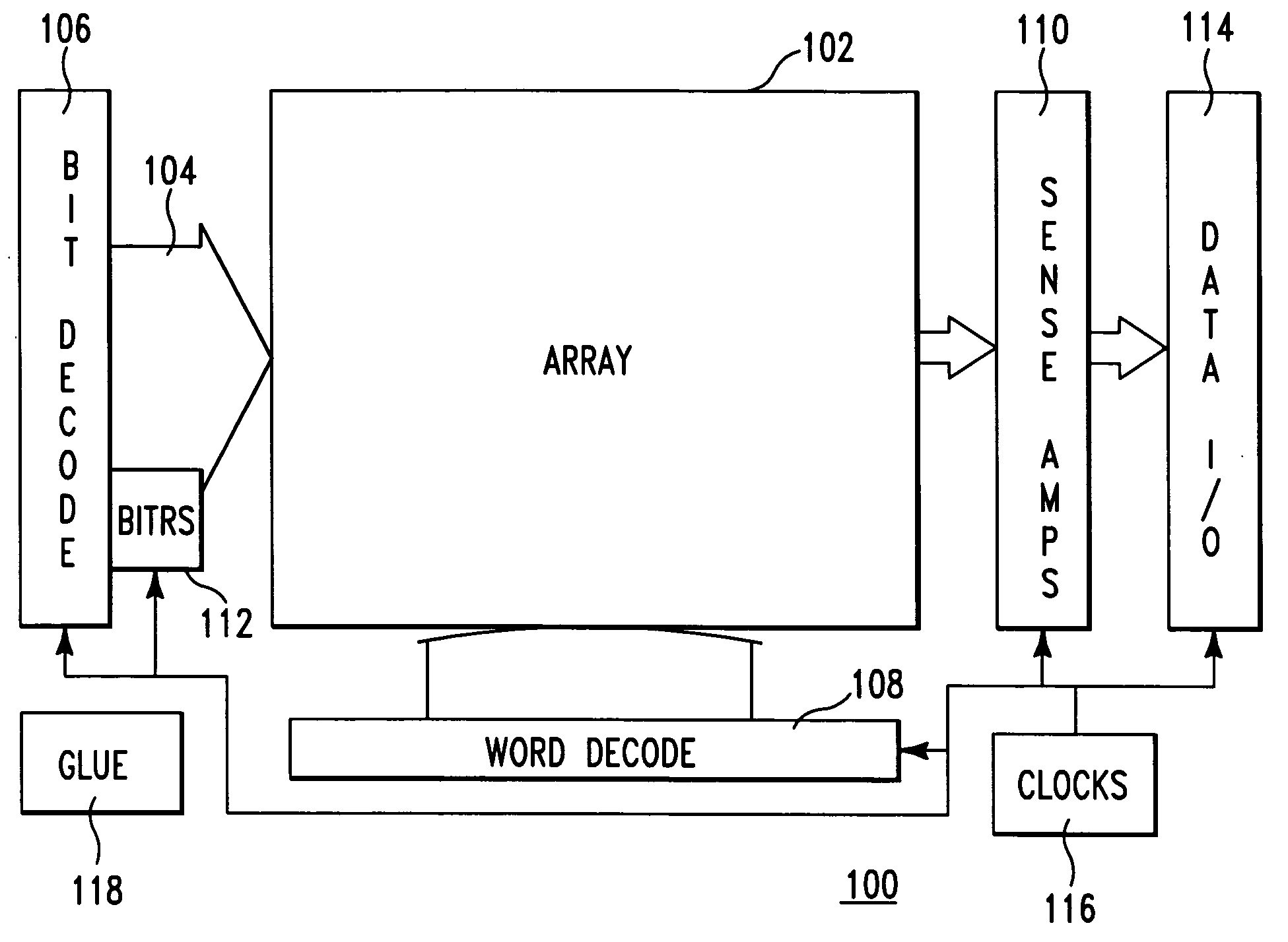
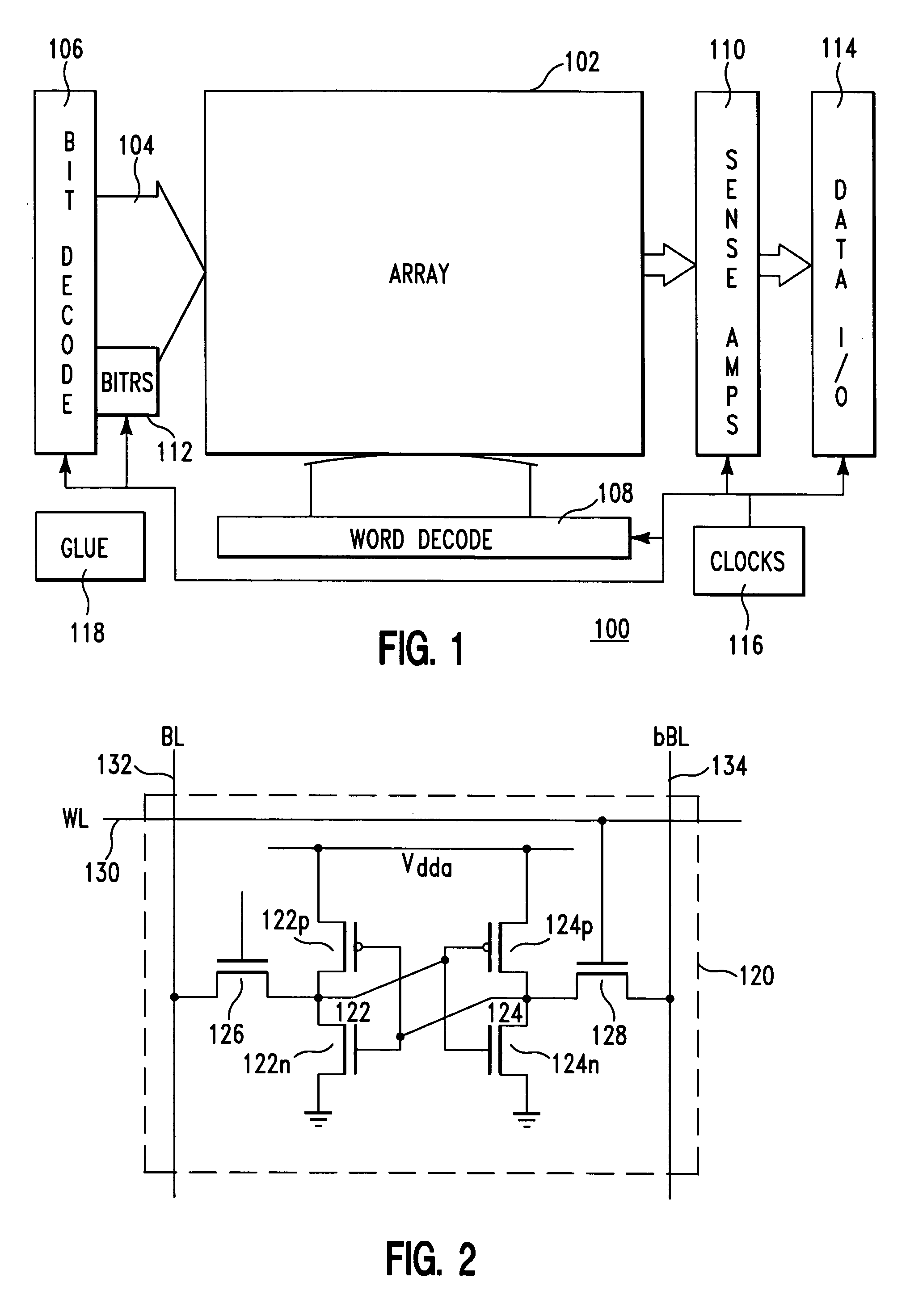
[0021] Turning now to the drawings and, more particularly, FIG. 1 shows a storage circuit 100 (e.g., memory), macro or chip, in the insulated gate technology known as CMOS, and more particularly, an array 102, subarray or array of subarrays of CMOS static random access memory (SRAM) cells. A column select 104 to the array 102 includes column restores that are pulsed off to float array columns when at least one column is being accessed to reduce the potential for half selected cell upsets for improved array stability according to a preferred embodiment of the present invention. While the present invention has application to improving stability in almost any array 102 of storage latches; the present invention is most advantageous to application in the any CMOS technology known as partially depleted (PD) silicon on insulator (SOI) technology that has a stated base design material or base design rule gate oxide thickness.
[0022] A bit decode circuit 106 decodes a bit address and selects one of N columns of cells in the array 102, an M by N array or subarray. A word decoder 108 selects one of M local word lines, each connected to a row of cells in the array 102. So, in this example, the array 102 is addressed by coincidence of a selected column with a selected row and cells in unselected columns on the selected row are half selected. Preferably, to keep bit line capacitance at optimum, the number of cells in each column is less than 100. The column select 104 also couples the selected cells to sense amplifiers 110 during a read to sense data stored in the selected cells. A bit restore float pulse generator 112 pulses the column restore at each column in the column select 104, to floats bit lines for half selected cells, i.e., for the duration of that pulse, preferably, which is, as long as the word decoder 108 is driving the selected word line. Data input/output (I/O) drivers 114 receive input data and drive sensed data from the sense amplifiers 110, e.g., off chip. Clock logic 118 provides local timing and glue logic 118 provides local control, e.g., read/write select, address gating and buffering, etc.
[0023]FIG. 2 shows an example of a preferred six transistor (6T) storage cell 120 or latch from an array 102 of such latches or cells 120. Data is stored in the cell 120 in a pair of cross coupled inverters 122, 124, accessed through a pair of pass gate FETs 126, 128. The gates of pass gate FETs 126, 128 are connected to a word line 130. In this 6T example each inverter 122, 124 includes an NFET 122N, 124N and a PFET 122P, 124P connected drain to drain and between array supply and ground. It should be noted that although the cell 120 of this example is a 6T cell, the present invention has application to any suitable single or multi port SRAM cell, e.g., an 8T or a 10T cell for improved stability in multi-ported SRAMs. For an example of such a multi port cell, see, U.S. Pat. No. 6,279,144 entitled “PROVABLY CORRECT STORAGE ARRAYS” to Henkels et al., issued Aug. 21, 2001, assigned to the assignee of the present invention and incorporated herein by reference.
[0024] Selecting the word line 130 turns on the pass gate FETs 126, 128 to selectively couple the cell contents to a pair of complementary bit lines 132, 134. Each word line 130 is connected to pass gates 126, 128 in a row of cells 120 and each pair of complementary bit lines 132, 134 is connected to a column of cells 120 in the array 102. Cell selection is by coincidence of a selected word line 130 with a selected bit line pair 132, 134. The cross coupled inverters 122, 124 are connected between an array voltage supply line and supply return or array ground. The bit line pair 132, 134 of a selected cell is floated during a read and driven to complementary levels (high and low or low and high) during a write. Previously, the bit line pairs 132, 134 were relatively large capacitive loads (e.g., several tenths of a picofarad) from connecting to a relatively large number of array rows. The columns were charged/clamped high (e.g., to Vdd) until selected and so, half selected cells 120 were biased to be in their most unstable state, enhancing the likelihood of upsets. By contrast, according to a preferred embodiment of the present invention, much shorter and so, much more lightly loaded bit line pairs 132, 134 of half selected cells are unclamped and allowed to float during every access. This allows the half selected cells to begin driving the floating bit line pair (i.e., pulling one side 132 or 134 low and allowing the other side 134, 132 to remain high) and, therefore, minimizes the likelihood of an upset.
[0025]FIG. 3 shows an example of a comparison of SRAM cell stability at different fabrication process points for cells 120 operating at 85° C. and over an array supply voltage (Vdd) range of 0.45 Volts (0.45V) to 2.25V. Normal variations in the fabrication process cause variations in device length, width and threshold (VT), which all determine cell stability. Accordingly, 6 different cell FET horizontal process points (width and length) are represented at each of 6 standard deviation (σ) points from nominal at the mean (0) to 5σ worst case in descending order and at five (5) different threshold standard deviation points from nominal to worst case, also in descending order. Essentially, data is written to the cells (1s and 0s); the cell word lines and bit lines 132, 134 are clamped high (i.e., half selected) for an selected period, e.g., clamped at Vdd at least a normal read or write access; and, the cell contents are read to determine if the data has been lost. Thus, fabrication process variations exacerbate cell instability, especially for the worst case cell length and width with the worst case VT, which could be considered unstable. However, floating lightly loaded bit lines for half selected cells according to the present invention, mitigates that instability.
[0026]FIG. 4A shows an example of a preferred column select driver 140, e.g., one of N in column select 104, for a complementary bit line pair 142, 144, connected to a number (M) of cells (not shown), each connected to one of M word lines in an M by N array 102. An inverter 146 receives a decoded column select signal 148 from the bit decode circuit 106. Bit line pull up devices, PFETs 150, 152, and equalization device, PFET 154 are on during standby and pulsed off when the word line is high by a bit restore signal (Bitrs) 156, which allows the bit line pair 142, 144 to float. The output of the inverter 146 is an input to a 2 input NOR gate 160 and drives a pair of bit line select pass gates, PFETs 162, 164. PFETs 162, 164 are read pass gates and during a read, pass a complementary signal on the selected bit line pair 142, 144 to a complementary data line pair 166, 168, respectively, that is connected to a sense amplifier (110 in FIG. 1). A write control signal 170 is a second input to the 2 input NOR gate 160. A pair of write devices, NFETs 172, 174, are driven by the output 176 of 2 input NOR gate 160. The write devices, NFETs 172, 174 selectively couple complementary input data on data write pair 178, 180 to bit line pair 142, 144, respectively.
[0027] In a typical access, an array word line (not shown) is driven high selecting a row of cells. Simultaneously or shortly thereafter, one selected column signal 148 rises at the input to the corresponding inverter 146 and the output of the inverter 146 falls to select the column. Simultaneously, or shortly thereafter, bit restore signal 156 pulses high to turn off all of the bit line pull up devices 150, 152 and equalization device 154, which floats all of the bit line pairs 142, 144, to allow a signal to develop. The capacitive load from the bit line pairs 142, 144 is light enough that, after a number of cycles, a full signal would develop on each half selected bit line pair 142, 144. Preferably, the pulse lasts as long as the selected word line is high. For the selected column the low on bit line select pass gates 162, 164 couples the bit line pair 142, 144 to the data line pair 166, 168. During a read, the write input 170 to NOR gate 160 remains high. So, the write devices 172, 174 remain off because the output 176 of NOR gate 160 is low. During a write, the write input 170 pulses low. So, the write devices 172, 174 turn on when the output of inverter 146 falls, which drives the output of NOR gate 160 high. With the write devices 172, 174 on, data passes from data write pair 172, 174 to the bit line pair 178, 180. During both a read and a write, PFETs 150, 152 and 154 in every column are pulsed off. Since half selected cells are not clamped to Vdd and a signal is allowed to develop on the bit line pair 142, 144, upsets are much less likely to occur even for cells with low threshold, short narrow devices.
[0028]FIG. 4B shows an example of a bit restore float pulse generator 190, e.g., 112 in the example of FIG. 1. A local clock (delclk1) 182 from clock logic 114 and bit addresses 184 are passed to a dynamic latch 192 that detects selection of a column. The dynamic latch 192 includes a n-way dynamic NOR gate 194, where n=log2 N, NORing n address bits 184 and an inverter 196. A reset PFET 198 gated by the clock 182, selectively resets the dynamic latch (pulling high the output of the n-way dynamic NOR gate 194 in an unaccessed subarray). An inverter 196 is cross coupled with the n-way dynamic NOR gate 194 through a clamping PFET 200. A buffer inverter 202 buffers the output of the dynamic latch 192. A pulse shaping latch 204 of cross coupled inverters 206, 208, latches the output of the buffer inverter 202. A pair of series inverters 210, 212, provides Bitrs 156 as the non-inverted delayed output of the buffer inverter 202. Four (4) series inverters 216, 218, 220, 222 provide a delayed output 224 of the inverted output of the pulse shaping latch 204.
[0029]FIG. 4C shows a timing example for the bit restore timer 190 of FIG. 4B. Normally, the clock 182 gating the reset PFET 198 is low. So, The reset PFET 198 is on, clamping the output of the n-way NOR gate 194 high. With the output of the n-way NOR gate 194 high, the output of the buffer inverter 202 and the non-inverted delayed output 156 are both low. Correspondingly, the inverted delayed output 224 is high. When the clock 182 rises, PFET 198 turns off, but the dynamic latch 192 maintains its current state, e.g., to compensate for an atypically slow access. When one or more bit addresses 184 rise, indicating that a column is being selected, the dynamic latch 192 is set and the output of the buffer inverter 202 rises. When the output of the buffer inverter 202 rises, the pulse shaping latch 104 switches states as the buffer inverter output 202 propagates through first series inverter 210. Thereafter, the non-inverted delayed output 156 rises two inverter stage delays after exiting the buffer inverter 202. Three inverter stage delays later, the inverted delayed output 224 falls. When the column selection has concluded and the high bit addresses 184 begin to fall, the dynamic latch 192 maintains its current state until the clock 182 falls. The clock falling turns on PFET 198 to reset the dynamic latch 192 and the output of the buffer inverter 202 falls. When the output of the buffer inverter 202 falls, the pulse shaping latch 104 switches states as the buffer inverter output 202 propagates through first series inverter 210. Thereafter, the non-inverted delayed output 156 falls, again two inverter stage delays after exiting the buffer inverter 202. Again, three inverter stage delays later, the inverted delayed output 224 rises.
[0030] FIGS. 5A-B show the improved cell stability for a preferred embodiment SRAM with the cell VT at 3σ worst case and the supply elevated to 0.1V above nominal. FIG. 5A shows a comparison of internal cell noise, e.g., in cell 120 of FIG. 2, i.e., on the internal storage nodes both with the bit lines 132, 134 clamped 230 to Vdd, and, unclamped 232 according to a preferred embodiment of the present invention. Advantageously, unclamping the bit lines 132, 134 for the half selected cell dramatically reduces internal cell noise. FIG. 5B shows a cell half select power comparison for same cell 120, with bit lines 132, 134 clamped 234 and, unclamped 236 according to a preferred embodiment of the present invention. Advantageously, half selected cells pulsed unclamped 234 deliver clear cut power savings, 5-6% per cell at 1.1 V, 85° C. in this example. Thus, pulsing the bit lines unclamped for half selected cells provides clear advantages both in power and stability for a preferred embodiment memory.
[0031] While the invention has been described in terms of preferred embodiments, those skilled in the art will recognize that the invention can be practiced with modification within the spirit and scope of the appended claims. It is intended that all such variations and modifications fall within the scope of the appended claims. Examples and drawings are, accordingly, to be regarded as illustrative rather than restrictive.