

Method for manufacturing dielectric thin film capacitor
a dielectric thin film capacitor and manufacturing method technology, applied in the direction of thin/thick film capacitors, stacked capacitors, discharge tubes luminescent screens, etc., can solve the problems of limited ti layer inevitably oxidizing, dielectric thin film cracking, and inability to obtain sufficient dielectric constan
- Summary
- Abstract
- Description
- Claims
- Application Information
AI Technical Summary
Benefits of technology
Problems solved by technology
Method used
Image

Examples
example
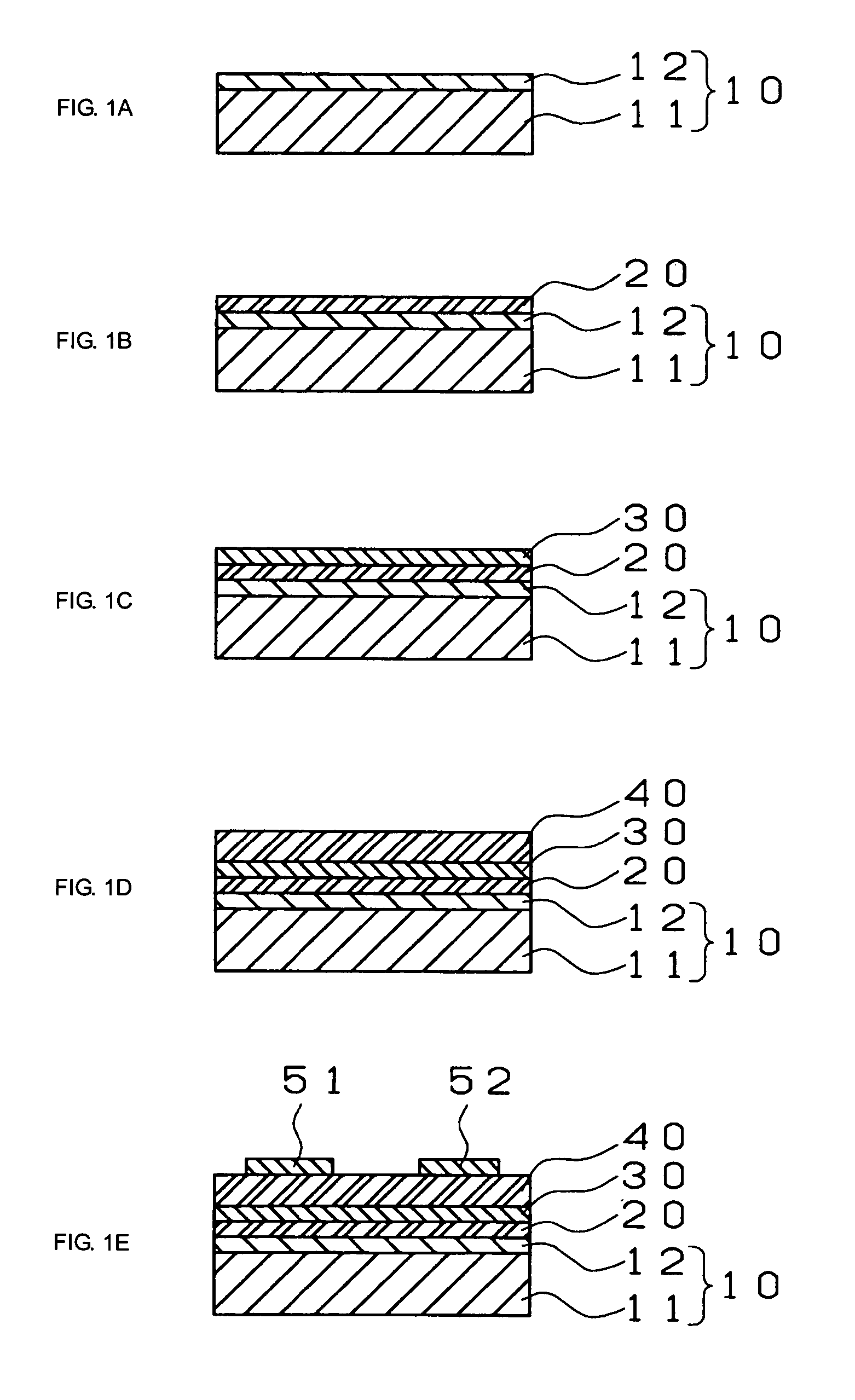
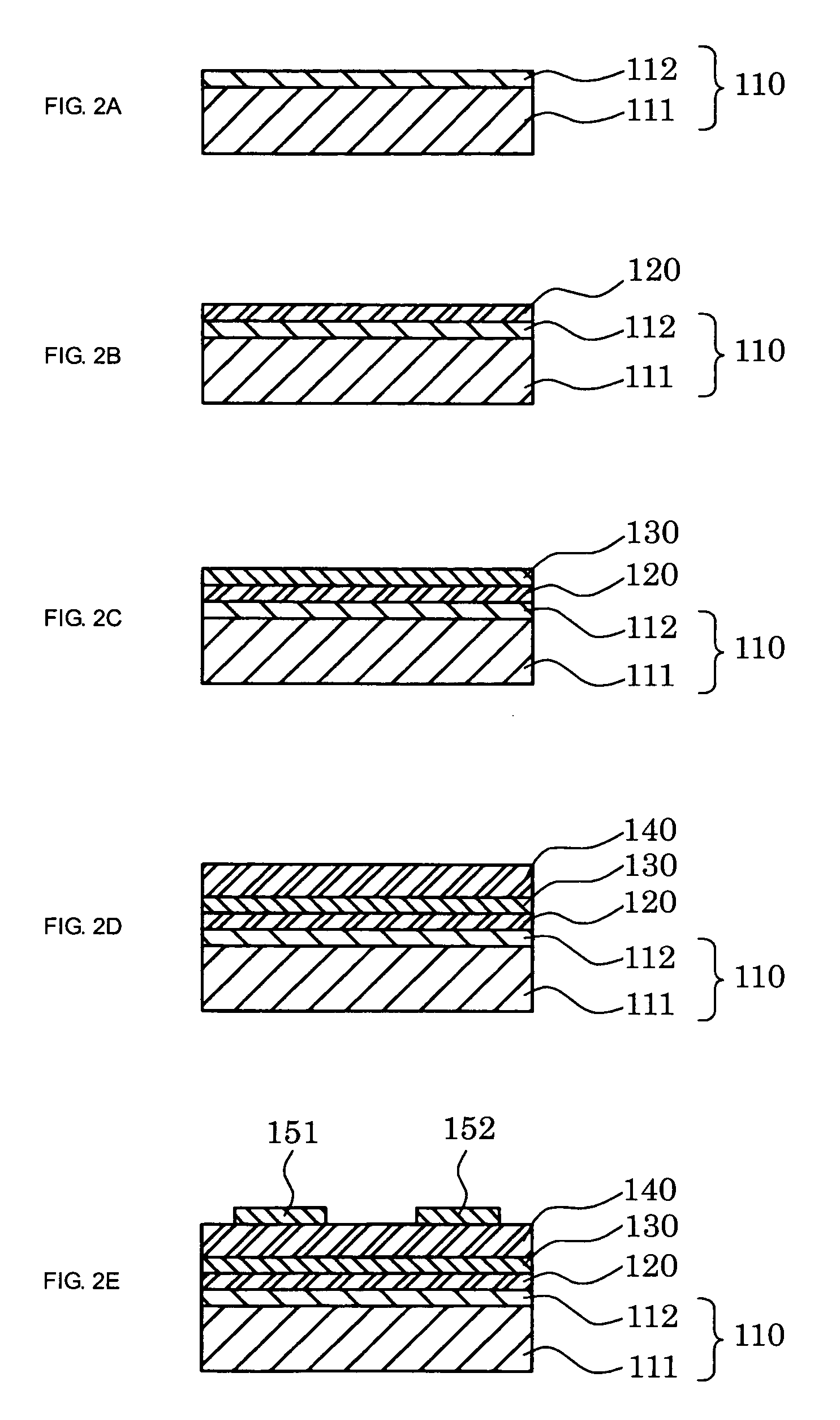
[0074] Examples of the present invention will be described in further detail below with reference to FIG. 2.
[0075] First, as shown in FIG. 2A, the substrate 110 comprising single crystal Si and having a diameter of 4 inches was prepared. The substrate 110 had a two-layer structure comprising the Si layer 111 and the SiO2 layer 112.
[0076] Next, a raw material solution containing an organic compound used as a raw material of BST was spin-coated on the substrate 110 and then dried on a hot plate. The spin-coating and drying were repeated several times each, and then a heat treatment was performed by a RTA (rapid thermal annealing) apparatus in an oxidizing atmosphere at 650° C. for 10 minutes to form the adhesive layer 120 comprising BST as shown in FIG. 2B.
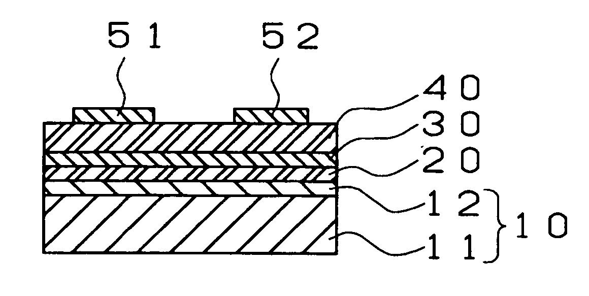
[0077] Next, the lower electrode 130 comprising Pt was formed on the adhesive layer 120 by a RF sputtering process as shown in FIG. 2C. If the lower electrode 130 has a large thickness, the equivalent series resistance of the die...
experiment 1
[0083] The first heat treatment of the above-described steps was performed for 30 minutes at a predetermined temperature of 550° C. to 700° C. to prepare a dielectric thin film capacitor, and the dielectric constant and tan δ of the dielectric thin film 140 were measured. The results are shown in Table 1. In Table 1, Sample Nos. #1 and #4 are comparative examples out of the range of the present invention, and a value of tan δ is a value measured at a frequency of 1 kHz.
TABLE 1Sam-TemperatureTemperature ofpleof first heatsecond heatDielectrictan δNo.treatment (° C.)treatment (° C.)constant(%)#15508006507.5#26008003902.1#36508003852.1#4700800NotNotMeasurableMeasurable
[0084] Table 1 indicates that in Sample No. #1 in which the temperature of the first heat treatment is 550° C., the dielectric constant is high, but the value of tan δ is undesirably high because the temperature of the first heat treatment is not more than about 50° C. higher than the crystallization temperature.
[0085]...
experiment 2
[0087] The second heat treatment of the above-described steps was performed for 30 minutes at a predetermined temperature of 700° C. to 850° C. to prepare a dielectric thin film capacitor, and the dielectric constant, tan δ, and the percent defective of the dielectric thin film 140 were measured. The results are shown in Table 2. In Table 2, Sample No. #5 is a comparative example out of the range of the present invention,,and the value of tan δ is a value measured at a frequency of 1 kHz. The percent defective represents the percent of defectives due to an initial short circuit.
TABLE 2TemperatureTemperatureofofPercentSamplefirst heatsecond heatDielectrictan δdefectiveNo.treatment (° C.)treatment (° C.)constant(%)(%)#56507002501.746#66507503251.74#76508003852.10#86508504204.22
[0088] Table 2 indicates that in Sample No. #5 in which the temperature of the second heat treatment is not more than about 100° C. higher than the temperature of the first heat treatment, the dielectric const...
PUM
 Abstract
Description
Claims
Application Information