Antenna switch

a technology which is applied in the direction of electrical equipment, radio transmission, transmission, etc., can solve the problems of antenna switch configuration, and achieve the effect of preventing increase in insertion loss, large effect, and complicated configuration of antenna switch

Inactive Publication Date: 2005-04-14
RENESAS TECH CORP
View PDF18 Cites 63 Cited by
  • Summary
  • Abstract
  • Description
  • Claims
  • Application Information

AI Technical Summary

Benefits of technology

[0012] Also in the circuit shown in FIG. 12, a switch is necessary for each receiving circuit. As the number of receiving circuits increases, the number of high handling voltage switches increases, and the configuration of the antenna switch becomes complicated. Further, to prevent increase in an insertion loss in multistage connection, a transistor having a large gate width is necessary as the high hand...

Problems solved by technology

As the number of kinds of operating frequencies increases, the number of transmission circuits to be added increases, and the configuration of the antenna switch becomes c...

Method used


Image

  • Antenna switch
  • Antenna switch
  • Antenna switch

Examples


first embodiment

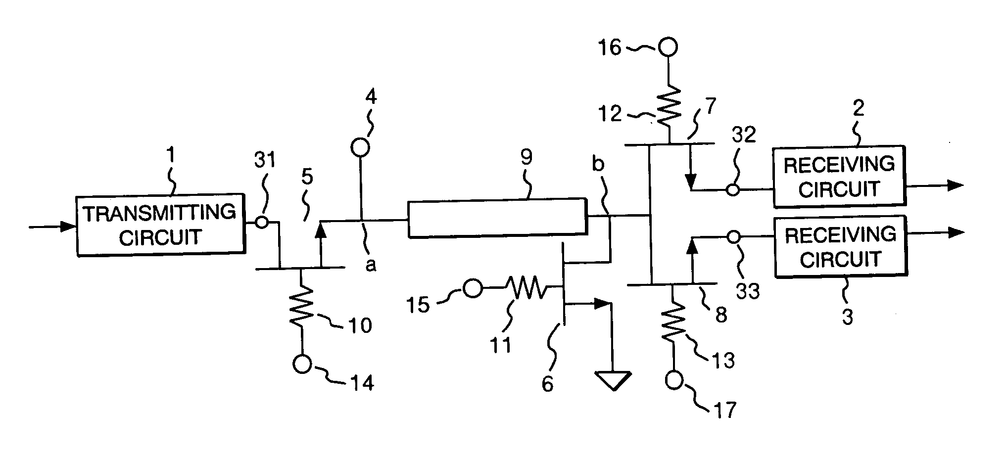
[0036] the invention will be described with reference to FIG. 1. FIG. 1 shows an antenna switch for switching connection among a transmitting circuit 1 handling a transmitted signal of a high output, two receiving circuits 2 and 3, and one antenna terminal 4.

[0037] A switching element 5 having one input and one output is connected between a transmitting terminal 31 for receiving an output signal of the transmitting circuit 1 and the antenna terminal 4. One end of a transmission circuit 9 is connected to the antenna terminal 4, and one end of a switch 6 having one input and one output is connected to the other end of the transmission circuit 9. The other end of the switch 6 is grounded. The length of the transmission circuit 9 is ¼ of the effective wavelength. The transmission circuit 9 turns the phase of a transmitted signal by 90 degrees at a frequency used. A switch 7 having one input and one output is connected between a receiving terminal 32 for supplying a received signal to th...

third embodiment

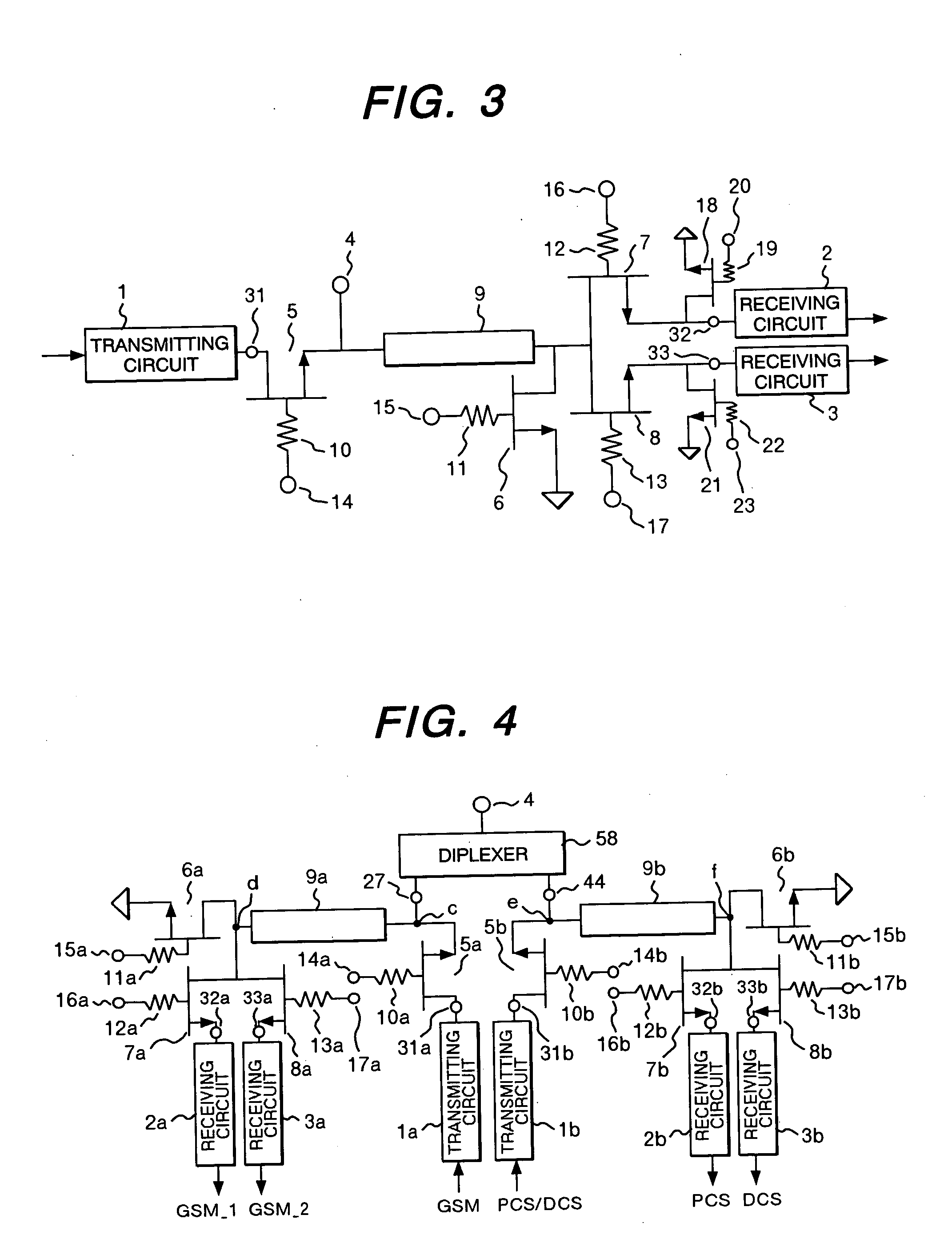
[0051] Specifically, the third embodiment relates to an antenna switch constructed between the antenna terminal 4 and a transmitting terminal 31a and receiving terminals 32a and 33a and between the antenna terminal 4 and a transmitting terminal 31b and receiving terminals 32b and 33b. The GSM terminal 27 and the PCS / DCS terminal 44 will be called sub antenna terminals and the antenna switch in FIG. 1 on the GSM side and the antenna switch in FIG. 1 on the PCS / DCS side will be called sub antenna switches. As reference numerals in for the sub antenna switch, reference numerals obtained by adding subscripts “a” and “b” to the reference numerals of FIG. 1 are used.

[0052] The length of a transmission circuit 9a is set to a length in which the phase of a transmitted signal is shifted by 90 degrees at the transmitting frequency of the GSM, and the length of a transmission circuit 9b is set to a length in which the phase of a transmitted signal is shifted by 90 degrees at the transmitting f...

sixth embodiment

[0076] The operation of the sixth embodiment performed at the time of transmitting / receiving in the PCS will be described as an example. At the time of receiving of PCS, the power amplifiers 112 and 114 are in the nonconductive state, the switches 126, 127, 129, 130, 132, and 133 are in the nonconductive state, and the switches 128 and 131 are in the conductive state. Consequently, a received signal which is input from the terminal 121 is supplied to the receiving circuit 119 via the switches 128 and 131 and the SAW filter 135 and demodulated, and the demodulated signal is output to the terminal 125.

[0077] At the time of transmitting in the PCS, since the operation frequencies overlap in a band from 1,850 MHz to 1875 MHz in PCS transmitting frequencies and DCS receiving frequencies, when a PCS transmitted signal in the band is output, the power supplied to an SAW filter 136 is determined by the isolation between the PCS transmitting and the DCS receiving. When isolation is insuffici...


PUM


Abstract

An antenna switch having a simple configuration and realizing high isolation between transmitting and receiving is provided. The antenna switch has a first switch connected between a transmitting terminal 31 and an antenna terminal 4, a transmission circuit 9 whose one end is connected to the antenna terminal and which shifts a phase of a transmitting signal by 90 degrees at use frequency, a second switch 6 whose one end is connected to the other end of the transmission circuit 9 and whose other end is grounded, and a plurality of third switches 7, 8 connected between the other end of the transmission circuit 9 and the plurality of receiving terminals 32, 33.

Description

CLAIM OF PRIORITY [0001] The present application claims priority from Japanese applications JP 2003-348990 filed on Oct. 8, 2003 and JP 2004-189257 filed on Jun. 28, 2004, the contents of which are hereby incorporated by reference into this application. FIELD OF THE INVENTION [0002] The present invention relates to an antenna switch for switching connection between a plurality of transmitting and receiving circuits and an antenna commonly used by the transmitting and receiving circuits. BACKGROUND OF THE INVENTION [0003] An antenna switch for switching connection between transmitting and receiving circuits handling a transmitted signal of a high output exceeding one watt and an antenna is strongly demanded to handle a high handling voltage and to have isolation between transmitting and receiving so that a transmitted signal is not leaked to a receiving circuit at the time of transmitting. [0004] An antenna switch addressing such requests is disclosed in Japanese Patent Laid-open No....

Claims


Application Information

Patent Timeline
IPC IPC(8): H04B1/44H04B1/48H01P1/15
CPCH04B1/48
Inventor OGAWA, TAKASHIKONDOH, HIROSHISUENAGA, HIDENORINAKAJIMA, AKISHIGE
Owner RENESAS TECH CORP
Why Eureka
Try Eureka