High efficiency nitride based light emitting device

a light emitting device and high-efficiency technology, applied in the direction of semiconductor devices, basic electric elements, electrical equipment, etc., can solve the problems of limited light emitted angle, light generated from leds is not easily emitted out, and improve the efficiency of light emission

Inactive Publication Date: 2005-04-21
EPISTAR CORP
View PDF6 Cites 207 Cited by
  • Summary
  • Abstract
  • Description
  • Claims
  • Application Information

AI Technical Summary

Benefits of technology

[0007] It is therefore a primary objective of the claimed invention to provide a nitride light emitting device and related method to solve the above-mentioned problem. The nitride light emitting device comprises a substrate; a first nitride semiconductor layer formed over the substrate, the first nitride semiconductor layer

Problems solved by technology

However, the light generated from an LED is not easily emitted out from the LED.
When LED light travels from a material with a high refractive index to the material with a low refractive index, the angle of light emitted is limited due to the effect of refractive indexes.
Therefore, an import

Method used


Image

  • High efficiency nitride based light emitting device
  • High efficiency nitride based light emitting device
  • High efficiency nitride based light emitting device

Examples


first embodiment

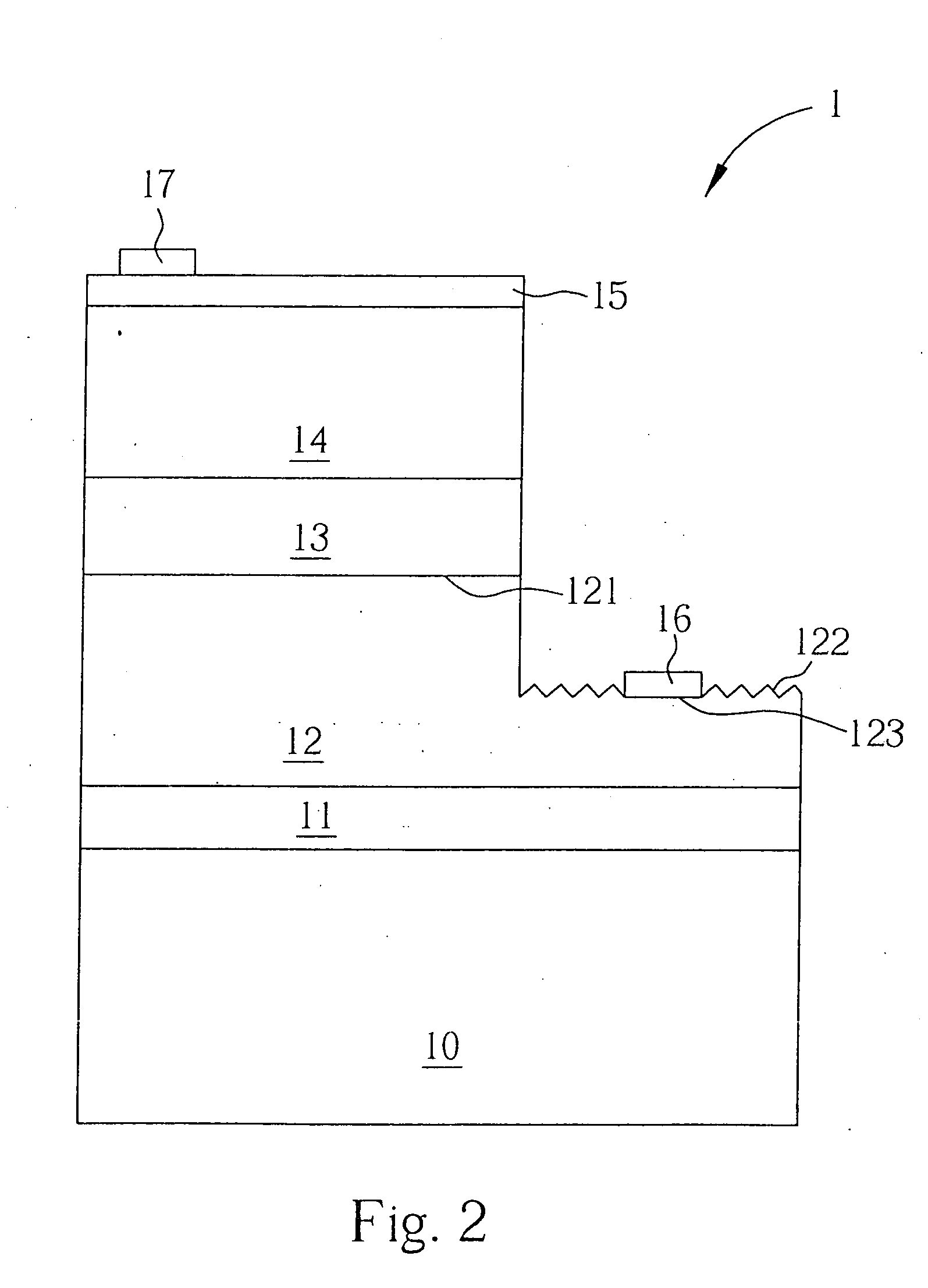
[0020] Please refer to FIG. 2. FIG. 2 illustrates the present invention nitride light emitting device 1. The nitride light emitting device 1 comprises a sapphire substrate 10; a nitride buffer layer 11 formed over the sapphire substrate 10; a N-type nitride semiconductor stack 12 formed over the nitride buffer layer 11, wherein an epitaxial surface 121, a rough surface 122, and a N-type contact area 123 are included on an upper surface of the N-type nitride semiconductor stack 12; a nitride multiple quantum-well structure emitting layer 13 formed over the epitaxial surface 121; a P-type nitride semiconductor stack 14 formed over the nitride multiple quantum-well structure emitting layer 13; a transparent conductive metal layer 15 formed over the P-type nitride semiconductor stack 14; a N-type electrode 16 formed over the N-type contact area 123; and a P-type electrode 17 formed over the transparent conductive metal layer 15.

[0021] There are many methods for manufacturing the nitride...

fourth embodiment

[0027] Please refer to FIG. 5. FIG. 5 illustrates the present invention nitride light emitting device 5. A key difference compared to the nitride light emitting device 4 is that an N-type reverse tunneling contact layer 59 with high concentration is formed between the P-type nitride semiconductor stack 14 and the transparent conductive oxide layer 49. The thickness of the N-type reverse tunneling contact layer 59 is less than 10 nm and the carrier concentration is more than 1*10{circumflex over ( )}19 cm{circumflex over ( )}−3. It is different to form a good Ohmic contact between the P-type nitride semiconductor stack 14 and the transparent conductive oxide layer 49, and thus forming the N-type reverse tunneling contact layer 59 with high concentration can form a good Ohmic contact to the transparent conductive oxide layer 49. When the LED is working under forward bias, the interface between the N-type reverse tunneling contact layer 59 and the P-type nitride semiconductor stack 14 ...

fifth embodiment

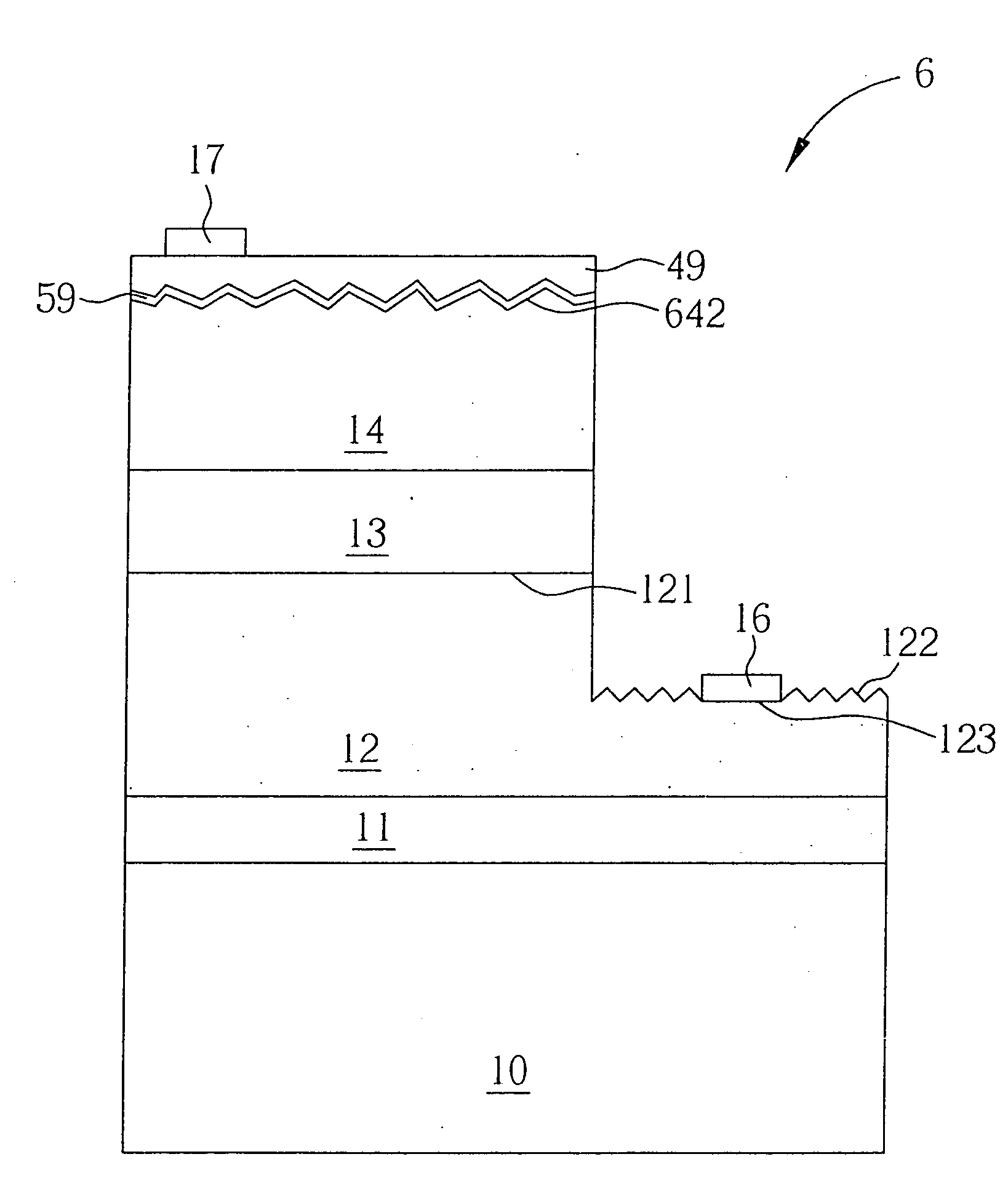
[0028] Please refer to FIG. 6. FIG. 6 illustrates the present invention nitride light emitting device 6. The nitride light emitting device 6 comprises the sapphire substrate 10; the nitride buffer layer 11 formed over the sapphire substrate 10; the N-type nitride semiconductor stack 12 formed over the nitride buffer layer 11, wherein the epitaxial surface 121, the rough surface 122, and the N-type contact area 123 are included on an upper surface of the N-type nitride semiconductor stack 12; the N-type electrode 16 formed over the N-type contact area 123; the nitride multiple quantum-well structure emitting layer 13 formed over the epitaxial surface 121; the P-type nitride semiconductor stack 14 formed over the nitride multiple quantum-well structure emitting layer 13, wherein a rough surface 642 is formed over the P-type nitride semiconductor stack 14; the N-type reverse tunneling contact layer 59 with high concentration formed over the P-type nitride semiconductor stack 14, wherei...


PUM


Abstract

A nitride light emitting device includes a substrate, a first nitride semiconductor stack formed above the substrate, the first nitride semiconductor stack having an epitaxial surface and a first rough surface, a distance from the epitaxial surface to the substrate being not less than a distance from the rough surface to the substrate, a nitride emitting layer formed on the epitaxial surface, and a second nitride semiconductor stack formed on the nitride emitting layer for promoting the efficiency of capturing light emitted from an LED.

Description

BACKGROUND OF INVENTION [0001] 1. Field of the Invention [0002] The present invention relates to a light emitting diode (LED) and related method, and more particularly, to a nitride light emitting device and related method. [0003] 2. Description of the Prior Art [0004] The light emitting diode (LED) has been widely used in various fields. For instance, light emitting diodes are capable of being installed in optical display devices, traffic lights, data storage devices, communication devices, illuminative equipment, and medical equipment. [0005] LED light travels in each direction instead of focusing on one place. However, the light generated from an LED is not easily emitted out from the LED. According to Snell's law, only light emitted at an angle within the critical angle θ c would be completely emitted out, and other light would be reflected and absorbed. In other words, the angle of LED light must be within a cone of 2 θ c to be completely emitted out. Light emitted at an angle ...

Claims


Application Information

Patent Timeline
IPC IPC(8): H01L33/22H01L33/32
CPCH01L33/32H01L33/22
Inventor OU, CHENCHEN, BIAU-DARWEY, SHANE-SHYANTSAI, YEN-TING
Owner EPISTAR CORP
Why Eureka
Try Eureka