

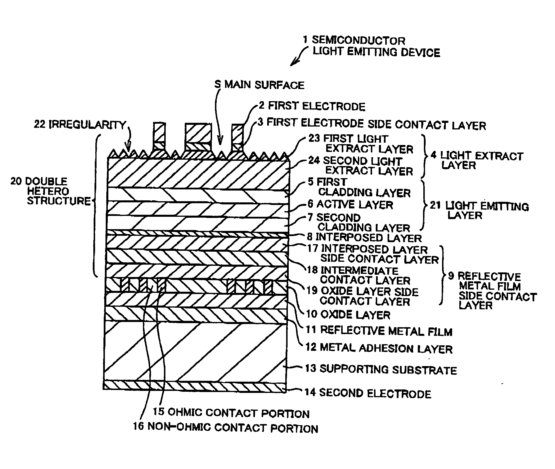
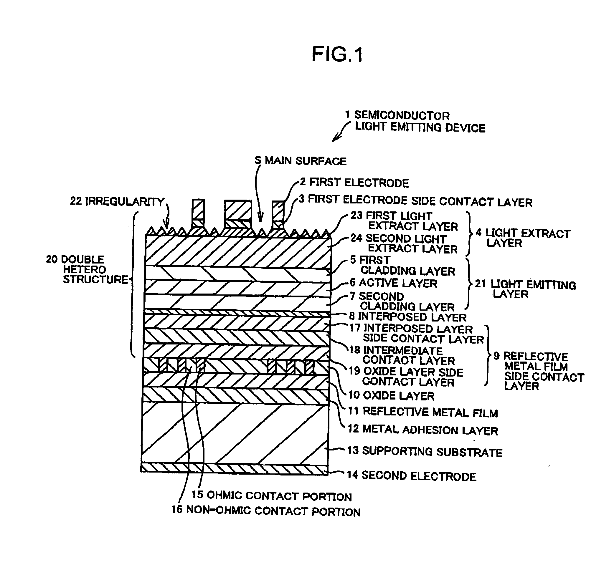
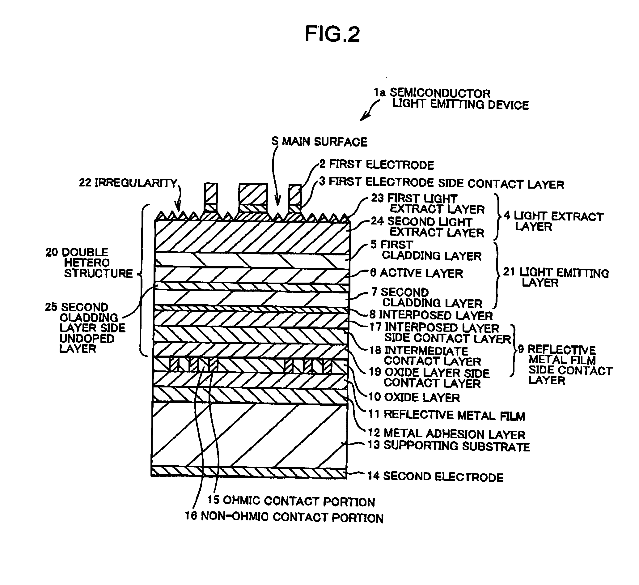
Semiconductor light emitting device
a technology of light-emitting devices and semiconductors, which is applied in the direction of semiconductor devices, basic electric elements, electrical appliances, etc., can solve the problems of difficult to improve the light-emitting efficiency enough, low light-emitting low efficiency of light-emitting devices to the outside, etc., to achieve the effect of superior effect and not reduced film thickness of light-emitting layers
- Summary
- Abstract
- Description
- Claims
- Application Information
AI Technical Summary
Benefits of technology
Problems solved by technology
Method used
Image

Examples
example 1
[0163]An epitaxial wafer for an LED namely for a red LED having a light emitting wavelength of around 630 nm, having a structure shown in FIG. 1 was manufactured. The detailed manufacturing process such as epitaxial growth process, film thickness of each epitaxial layer, structure and material of each epitaxial layer, structure of a reflective metal film, structure and dimensions of an ohmic contact portion, method of re-sticking to the supporting substrate, method of forming electrodes, method of etching is as follows.
[0164]As shown in FIG. 10, on an n-type GaAs substrate (substrate for growth) 41, an n-type (Se-doped) (Al0.7Ga0.3)0.5In0.5P etching stopper layer (a film thickness of 200 nm and a carrier concentration of 1×10¹⁸ / cm3) (etching stopper layer) 42, an n-type (Se-doped) GaAs contact layer (a film thickness of 50 nm and a carrier concentration of 1×10¹⁸ / cm3) (first electrode side contact layer) 3, an n-type (Se-doped) (Al0.7Ga0.3)0.5In0.5P window layer (a film thickness of...
example 2
[0190]An epitaxial wafer for an LED namely for a red LED having a light emitting wavelength of around 630 nm, having a structure shown in FIG. 8 was manufactured. The detailed manufacturing process such as epitaxial growth process, film thickness of each epitaxial layer, structure and material of each epitaxial layer, structure of a reflective metal film, structure and dimensions of an ohmic contact portion, method of re-sticking to the supporting substrate, method of forming electrodes, method of etching is as follows.
[0191]As shown in FIG. 10, on an n-type GaAs substrate (substrate for growth) 41, an n-type (Se-doped) (Al0.7Ga0.3)0.5In0.5P etching stopper layer (a film thickness of 200 nm and a carrier concentration of 1×10¹⁸ / cm3) (etching stopper layer) 42, an n-type (Se-doped) GaAs contact layer (a film thickness of 50 nm and a carrier concentration of 1×10¹⁸ / cm3) (first electrode side contact layer) 3, an n-type (Se-doped) (Al0.4Ga0.6)0.5In0.5P window layer (a film thickness of...
example 3
[0203]An epitaxial wafer for an LED namely for a red LED having a light emitting wavelength of around 630 nm, having a structure shown in FIG. 9A was manufactured. The detailed manufacturing process such as epitaxial growth process, film thickness of each epitaxial layer, structure and material of each epitaxial layer, structure of a reflective metal film, structure and dimensions of an ohmic contact portion, method of re-sticking to the supporting substrate, method of forming electrodes, method of etching is in principle similar to that in the Example 2. Next, only the points different from the Example 2 will be explained in more detail.
[0204]The light extract layer 4a comprises a first light extract layer 23b, a second light extract layer 24b and a third light extract layer 27. The first light extract layer 23b comprises an n-type (Se-doped) (Al0.4Ga0.6)0.5In0.5P window layer (a film thickness of 400 nm and a carrier concentration of 1×10¹⁸ / cm3), the second light extract layer 24b...
PUM
 Abstract
Description
Claims
Application Information