Solid-state imaging device, pixel-signal processing method, analog-signal transferring device, and analog-signal transferring method

a solid-state imaging and processing method technology, applied in the direction of color television details, television systems, radio control devices, etc., can solve the problems of unfavorable analog-signal transferring, high power consumption, and complex systems, and achieve the effect of favorable analog-signal transferring

Inactive Publication Date: 2005-04-21
SONY CORP
View PDF4 Cites 30 Cited by
  • Summary
  • Abstract
  • Description
  • Claims
  • Application Information

AI Technical Summary

Benefits of technology

[0028] In view of the situation described above, it is an object of the present invention to provide a favorable solid-state imaging device and a pixel-signal processing method, i.e., to provide a circuit that gives tracking ability for a black level at low power consumption without causing increase in layout area in an arrangement in which charge integrating amps are provided for the respective columns. It is another object of the present invention to provide a favorable analog-signal transferring device and analog-signal transferring method.

Problems solved by technology

The problems of CCD image sensors include, for example, the problem that CCD requires special processes for manufacturing, the problem that a plurality of power supply voltages is needed for operation thereof, and the problem that the system is very complex since a plurality of peripheral ICs must be used in combination.
According to Japanese Unexamined Patent Application Publication No. 5-207220, since amps must be provided for the respective columns, power consumption inevitably increases.
This causes increase in operation current per one amp among the amps provided for the respective columns, causing additional increase in power consumption.
Furthermore, although the reference voltage Vref essentially determines the black level of signals, since a fixed potential is used, tracking ability to variation factors such as temperature change or power supply voltage is not provided.
Thus, compared with the example described in Japanese Unexamined Patent Application Publication No. 5-207220, the amps must operate at a very high speed, causing increase in current that flows per one amp.
Furthermore, the layout area of the amps increases, which is very disadvantageous considering the restriction that the amps must be laid out respectively for the vertical signal lines from the imaging pixel array, i.e., for the respective columns, so that difficulty is design is expected.

Method used


Image

  • Solid-state imaging device, pixel-signal processing method, analog-signal transferring device, and analog-signal transferring method
  • Solid-state imaging device, pixel-signal processing method, analog-signal transferring device, and analog-signal transferring method
  • Solid-state imaging device, pixel-signal processing method, analog-signal transferring device, and analog-signal transferring method

Examples


first embodiment

[0081] First Embodiment

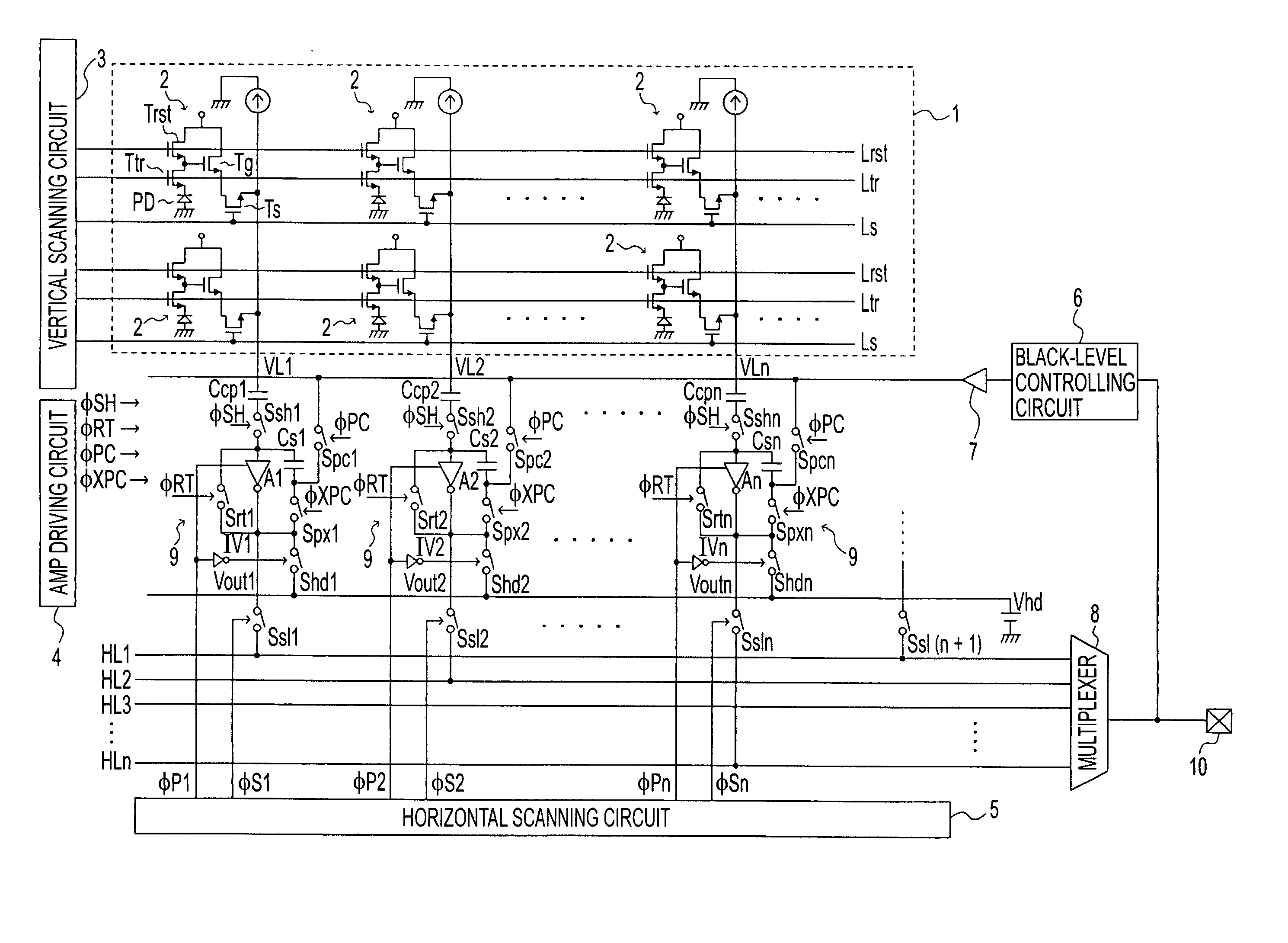
[0082]FIG. 1 shows a construction according to a first embodiment of the present invention. The circuit shown in FIG. 1 allows pixel signals obtained by a pixel array 1 in a solid-state imaging device to be output from an output terminal 10. A lens system for forming a path of light incident on the pixel array 1 and a signal processing system provided at a subsequent stage of the output terminal 10 are not shown, and descriptions thereof will be omitted.

[0083] The pixel array 1 includes a large number of imaging pixels 2 arranged in a row direction and a column direction. Each of the pixels 2 is formed by a photodiode PD, a transferring transistor Ttr, a reset transistor Trst, an amplifying transistor Tg, and a selecting transistor Ts, connected as shown in FIG. 1.

[0084] The selecting transistors Ts of the imaging pixels 2 on each column of the pixel array 1 are commonly connected to a vertical signal line VL (VL1, VL2, . . . VLn).

[0085] Furthermore, in ord...

second embodiment

[0191] Second Embodiment

[0192]FIG. 8 shows a construction according to a second embodiment of the present invention. In the following description of embodiments, parts corresponding to those in FIG. 1 are designated by the same numerals, and descriptions thereof will be omitted.

[0193] The construction shown in FIG. 8 is basically the same as that of the first embodiment shown in FIG. 1, but differs in that signals φS (φS1, φS2, . . . ) output from the horizontal scanning circuit 5 are commonly used as amp controlling signals and amp selecting signals.

[0194] That is, the horizontal scanning circuit 5 supplies the signals φS to control standby of the amps A and to control the switches Shd.

[0195] In the first embodiment described above, the amp controlling signals φP are caused to rise somewhat earlier than the amp selecting signals φS in consideration of the time for the amps A to return from the standby state, as described with reference to FIG. 2. If the amps A do not take much t...

third embodiment

[0199] Third Embodiment

[0200]FIG. 11 shows a third embodiment of the present invention. In this embodiment, feedback capacitors Csv (Csv1, Csv2, . . . ) of the amps A in the charge integrating amps 9 are implemented by variable capacitors.

[0201] Thus, the term Ccp / Cs in equation (1) becomes variable, so that variable-gain amplifiers are implemented.

[0202] It is to be readily understood that the variable capacitors Cvs can be implemented by allowing selection from a plurality of capacitors by switches. In that case, pulses for selecting capacitance are output from the amp driving circuit 4.

[0203] According to the third embodiment, the function of programmable gain amp (PGA), which is required in a camera system, can be implemented in the charge integrating amps 9. Thus, systems at subsequent stages can be simplified, and the gain is increased at an early stage. Accordingly, sufficient signal amplitude is ensured even when pixel signal levels are small, and insusceptibility to nois...


PUM


Abstract

From a pixel array where imaging pixels are arranged, pixel signals of respective columns on a selected row are read in parallel in a horizontal blanking period of a horizontal period. The pixel signals of the respective columns are output to horizontal signal lines in an effective period of the horizontal period via charge integrating amps provided respectively for the columns, i.e., provided respectively for vertical signal lines, and are thereby transferred horizontally. In the charge integrating amps, it is possible to enter a standby state while holding the pixel signals by a holding voltage. Furthermore, in the charge integrating amps, a reference potential for precharging feedback capacitors for amps at the time of a reading operation is automatically controlled based on a black level. Furthermore, pixel signals from the respective charge integrating amps are horizontally transferred in parallel using a plurality of horizontal signal lines.

Description

BACKGROUND OF THE INVENTION [0001] 1. Field of the Invention [0002] The present invention relates to a solid-state imaging device, a pixel-signal processing method for a solid-state imaging device, an analog-signal transferring device, and an analog-signal transferring method. [0003] 2. Description of the Related Art [0004] Recently, as an alternative to CCD image sensors, interest in CMOS image sensors has arisen. This is because CMOS image sensors overcome various problems of CCD image sensors. The problems of CCD image sensors include, for example, the problem that CCD requires special processes for manufacturing, the problem that a plurality of power supply voltages is needed for operation thereof, and the problem that the system is very complex since a plurality of peripheral ICs must be used in combination. [0005] CMOS image sensors can be manufactured by the same manufacturing processes as ordinary CMOS integrated circuits that are manufactured around the world. Furthermore, ...

Claims


Application Information

Patent Timeline
Patent Type & Authority Applications(United States)
IPC IPC(8): H04N5/335H01L27/146H04N5/341H04N5/361H04N5/369H04N5/374H04N5/376H04N5/378
CPCH04N5/378H04N25/75H04N25/74H04N25/77
Inventor KOSEKI, KENHARUTA, TSUTOMU
Owner SONY CORP
Why Eureka
Try Eureka