

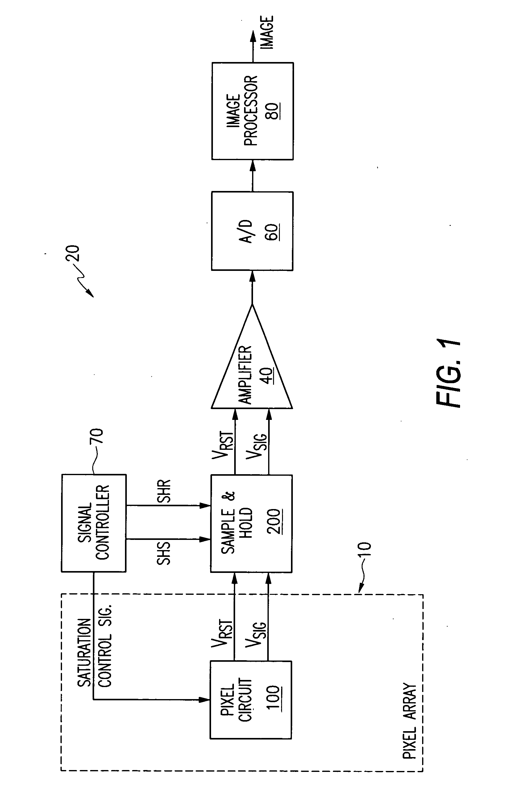
Dynamic range enlargement in CMOS image sensors
a dynamic range and image sensor technology, applied in the field of dynamic range enlargement in cmos image sensors, can solve the problems of large variation in the represented signal, slow response of the log portion of the circuit, and difficulty in control, so as to increase the intrascene dynamic range for image capture and reduce the photo-conversion gain of the pixel circui
- Summary
- Abstract
- Description
- Claims
- Application Information
AI Technical Summary
Benefits of technology
Problems solved by technology
Method used
Image

Examples
first embodiment
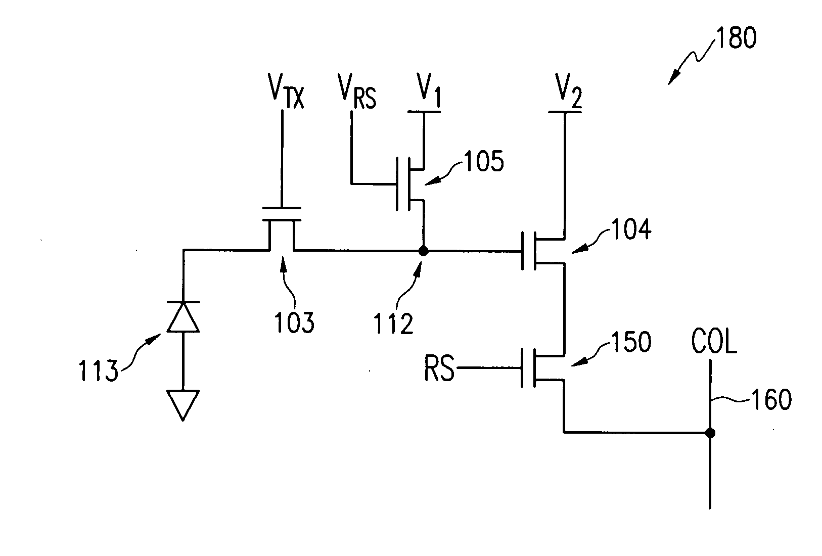
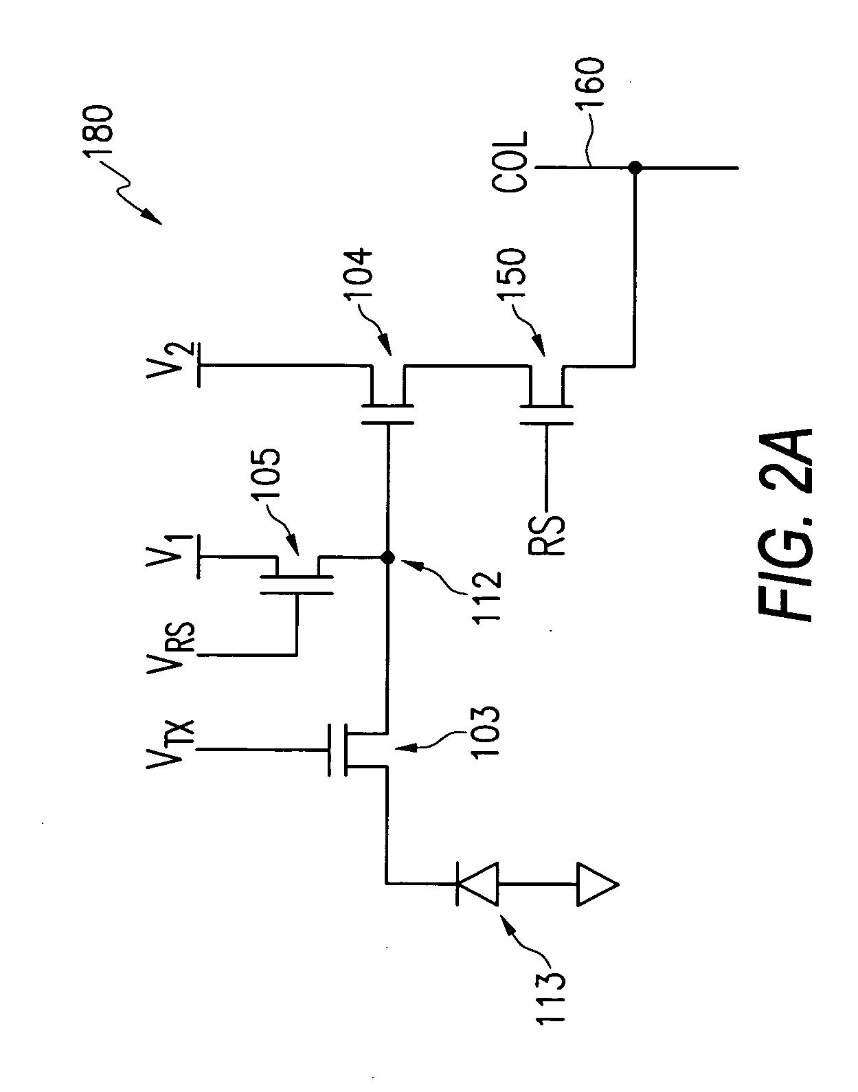
[0026]FIG. 2B illustrates an exemplary cross-section 100 of a portion of the four-transistor (4-T) pixel circuit of FIG. 2A, along with a related potential diagram 120 and signal level transfer diagram 130 in accordance with the invention. The cross-section 100 illustrates a buried photodiode region 113 comprising a p-type region 101 and an n-type region 102, which serves as a photodiode where photocharge is generated and accumulated until transferred. Adjacent to the buried photodiode region 113 is a transfer transistor 103, which receives a saturation control signal (VTX) 112 as shown in FIG. 2B. Next to the transfer transistor 103 is a floating diffusion region 112, which is coupled to the gate of the source-follower transistor 104. Reset transistor 105 operates to reset the floating diffusion region 112 prior to the transfer of charge from the photodiode 113. Reset transistor 105 supplies a reset voltage at the diffusion region 112 when the VRS signal is high.
[0027]FIG. 2B also ...
second embodiment
[0034]FIG. 4A illustrates an exemplary schematic of a five-transistor (5-T) pixel circuit 280 in accordance with the present invention. Generally, pixel circuit 280 includes a photodiode 240 that accumulates photocharge during an integration period. The photodiode 240 is coupled to a drain terminal of anti-blooming transistor 214, whose source terminal is coupled to operating voltage (V1). A gate terminal of anti-blooming transistor 214 receives saturation control signal (VABST), which is discussed in greater detail below. Photodiode 240 is also coupled to transfer transistor 204, which receives a transfer signal (VTX) at a gate terminal to allow charge to transfer from the photodiode 240 to a floating diffusion node 220. A source terminal of transfer transistor 204 is coupled to floating diffusion node 220, which further couples to a drain terminal of reset transistor 206. Reset transistor 206 receives a reset signal (RST) at a gate terminal to activate the transistor 206 to reset ...
third embodiment
[0041]FIG. 6A is an exemplary schematic of a two-transistor (2-T) shared floating diffusion node pixel circuit 580 under the invention. Generally, circuit 580 has two photodiodes 503, 512 which are respectively coupled to a the source terminals of respective transfer transistors 505, 515. Each transfer transistor (505, 515) is activated by a respective saturation control signals (TX-A, TX-B), the operation of which is described in greater detail below. Each saturation control signals TX-A, TX-B is applied to a gate terminal of a respective transistor as shown in FIG. 6A. The drain terminals of the transfer transistors 505, 515 are both coupled to a common floating diffusion node 509, which is further coupled to a gate terminal of source-follower transistor 506, and a drain terminal of reset transistor 507. The reset transistor 507 receives a reset pulse RST at the gate terminal to clear out charge from floating diffusion region 509, and has a source terminal coupled to operating vol...
PUM
 Abstract
Description
Claims
Application Information