ESD protection for integrated circuits

a protection device and integrated circuit technology, applied in the direction of semiconductor devices, electrical apparatus, transistors, etc., can solve the problems of affecting device operation, affecting the operation of integrated circuits, and continuing problems such as esd

Inactive Publication Date: 2005-04-21
TEXAS INSTR INC
View PDF13 Cites 35 Cited by
  • Summary
  • Abstract
  • Description
  • Claims
  • Application Information

AI Technical Summary

Benefits of technology

[0007] The following presents a simplified summary of the invention in order to provide a basic understanding of some aspects of the invention. This summary is not an extensive overview of the invention. It is intended to neither identify

Problems solved by technology

Electrostatic discharge (ESD) is a continuing problem in the design and manufacture of semiconductor devices.
Integrated circuits (ICs) can be damaged by ESD events, in which large currents flow through the device.
Such ESD current can flow from the pad to ground through vulnerable circuitry in the IC that m

Method used


Image

  • ESD protection for integrated circuits
  • ESD protection for integrated circuits
  • ESD protection for integrated circuits

Examples


Embodiment Construction

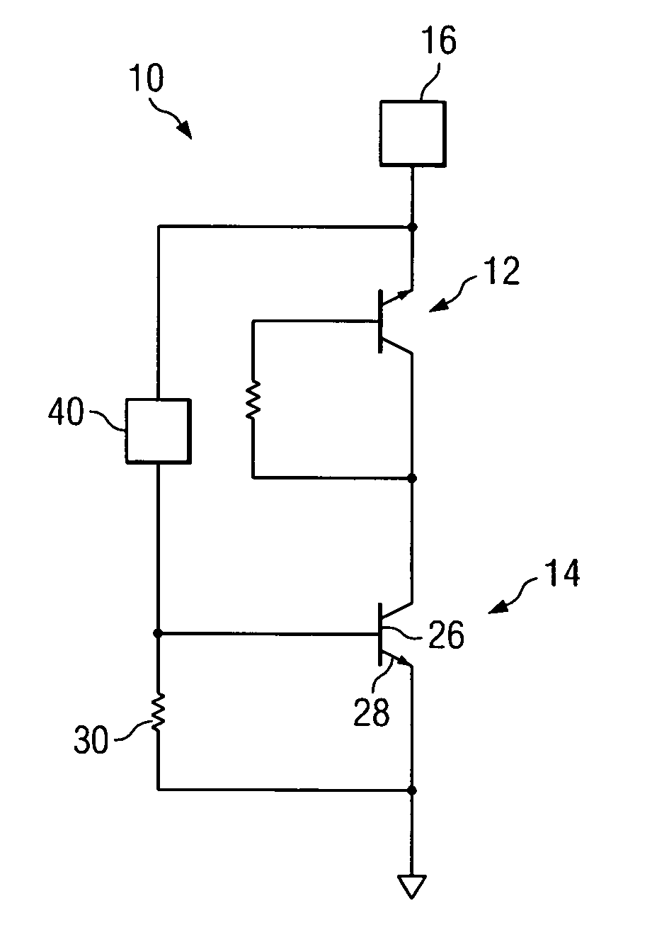
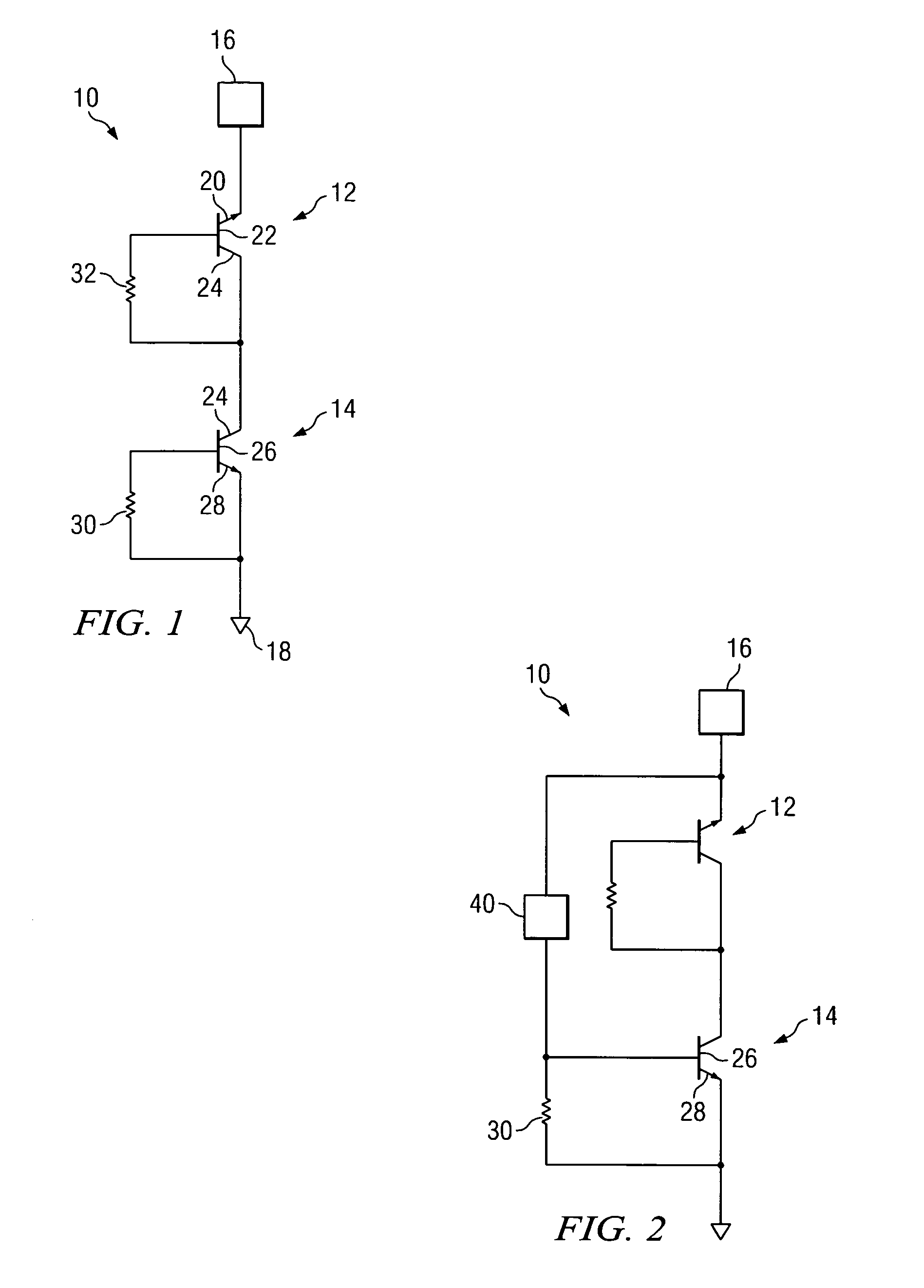
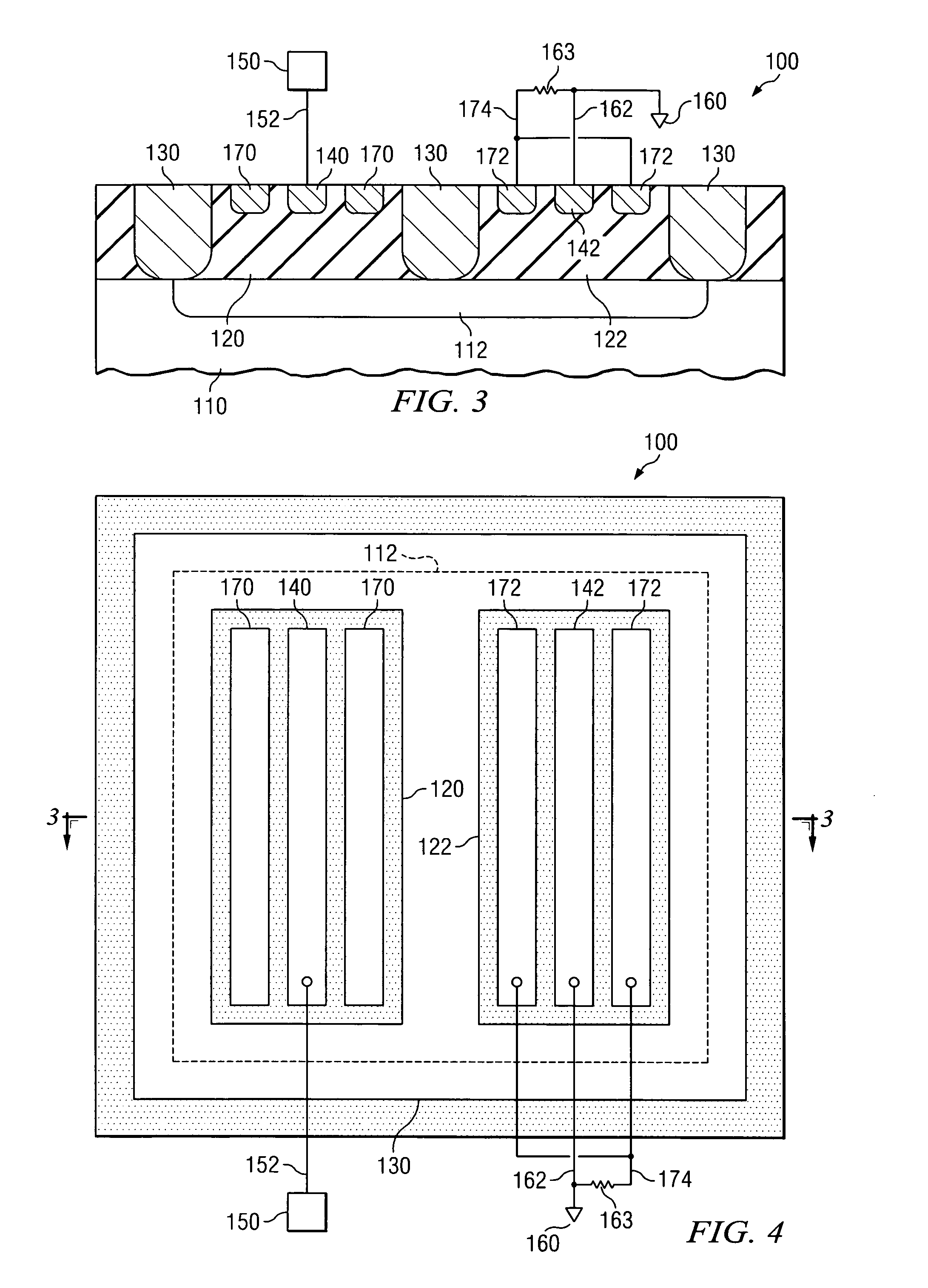
[0023] The present invention relates generally to an ESD protection device and methods for making such a device. The ESD protection device includes two bipolar npn transistors that are coupled in series for use in clamping applications. The first bipolar npn transistor and the second bipolar npn transistor can share a common collector. By sharing a common collector, a high voltage (e.g., greater than about 15 volts) ESD protection device can be provided in which the resistance is minimized, for example, to less than about 2 ohms. Additionally, an ESD protection device with a common collector can occupy less area (e.g., about two times less) as well as have a reduced parasitic capacitance and leakage compared to two separate bipolar npn transistors, which do not share a common collector.

[0024]FIG. 1 illustrates a schematic circuit design of an ESD protection device 10 in accordance with one aspect of the present invention. The ESD protection device 10 includes a first bipolar npn tr...


PUM


Abstract

An ESD protection device includes two bipolar npn transistors that are coupled in series for use in clamping applications. The emitter of the first bipolar transistor can be coupled to a protected node and the emitter of the second bipolar transistor can be coupled to a grounded node. The first bipolar transistor and the second bipolar transistor can share a common collector.

Description

TECHNICAL FIELD [0001] The present invention relates generally to protection devices for integrated circuits, and more particularly to a device for protecting integrated circuits from electrostatic discharge (ESD). BACKGROUND OF THE INVENTION [0002] Electrostatic discharge (ESD) is a continuing problem in the design and manufacture of semiconductor devices. Integrated circuits (ICs) can be damaged by ESD events, in which large currents flow through the device. These ESD events can stem from a variety of sources. In one such ESD event, a packaged IC acquires a charge when it is held by a human whose body is electrostatically charged. An ESD event can occur when the IC is inserted into a socket, and one or more of the pins of the IC package touch the grounded contacts of the socket. This type of event is known as a human body model (HBM) ESD event. For example, a charge of about 0.6 μC can be induced on a body capacitance of 150 pF, leading to electrostatic potentials of 4 kV or great...

Claims


Application Information

Patent Timeline
IPC IPC(8): H01L27/02H01L29/732H02H9/00
CPCH01L29/7322H01L27/0259
Inventor STEINHOFF, ROBERT M.BRODSKY, JONATHAN S.
Owner TEXAS INSTR INC
Why Eureka
Try Eureka