Sub-micron-scale patterning method and system

a micro-scale patterning and micro-scale technology, applied in the field of sub-micron-scale patterning method and system, can solve the problems of limited nano-scale pattern transfer, inability to create nano-scale patterns, and inability to achieve the effect of forming nano-scale patterns, and achieve good film uniformity and controlled thickness

Inactive Publication Date: 2005-04-21
WANG JIAN +2
View PDF7 Cites 78 Cited by
  • Summary
  • Abstract
  • Description
  • Claims
  • Application Information

AI Technical Summary

Benefits of technology

[0008] A method for replicating a nanopattern is disclosed. This method includes identifying a substrate; coating a surface of the substrate with a liquid layer with controlled thickness and good film uniformity; positioning a mold having a plurality of recesses defining a negative of the nanopattern in sufficient proximity with the coated liquid layer to cause the liquid layer to self-fill at least a portion of the plurality of recesses of the mold; and, chemically transforming the liquid layer to enable the transformed film to substantially retain the nanopattern.

Problems solved by technology

While each of these methods differs in the specific method and steps, or physical principle, the methods all suffer from drawbacks in forming nano-scale patterns.
While embossing generally produces a uniform pattern and provides relatively easy mold separation, embossing generally has several drawbacks with respect to the creation of nano-scaled devices.
Embossing occurs at a high or at least elevated temperature, involves high pressure, acts on bulk structures, and results in limited nano-scale pattern transfer.
Each of these drawbacks lessens the usefulness of embossing for creation nano-scale patterns.
While injection molding produces uniform patterns and provides easy mold separation, injection molding suffers from many drawbacks in creating nano-scaled device.
For example, injection molding requires elevated temperatures, high pressure, bulk structures, and results in limited pattern transfer at the nano-scale.
These drawbacks reduce the usefulness of injection molding in creating nano-scale patterns.
While step and flash imprinting may be performed at room temperatures and provide easy mold separation, step and flash imprint suffers from many drawbacks with respect to nano-scale patterns.
Step and flash imprint requires low to medium pressure levels and often produces a non-uniform pattern.

Method used


Image

  • Sub-micron-scale patterning method and system
  • Sub-micron-scale patterning method and system
  • Sub-micron-scale patterning method and system

Examples


Embodiment Construction

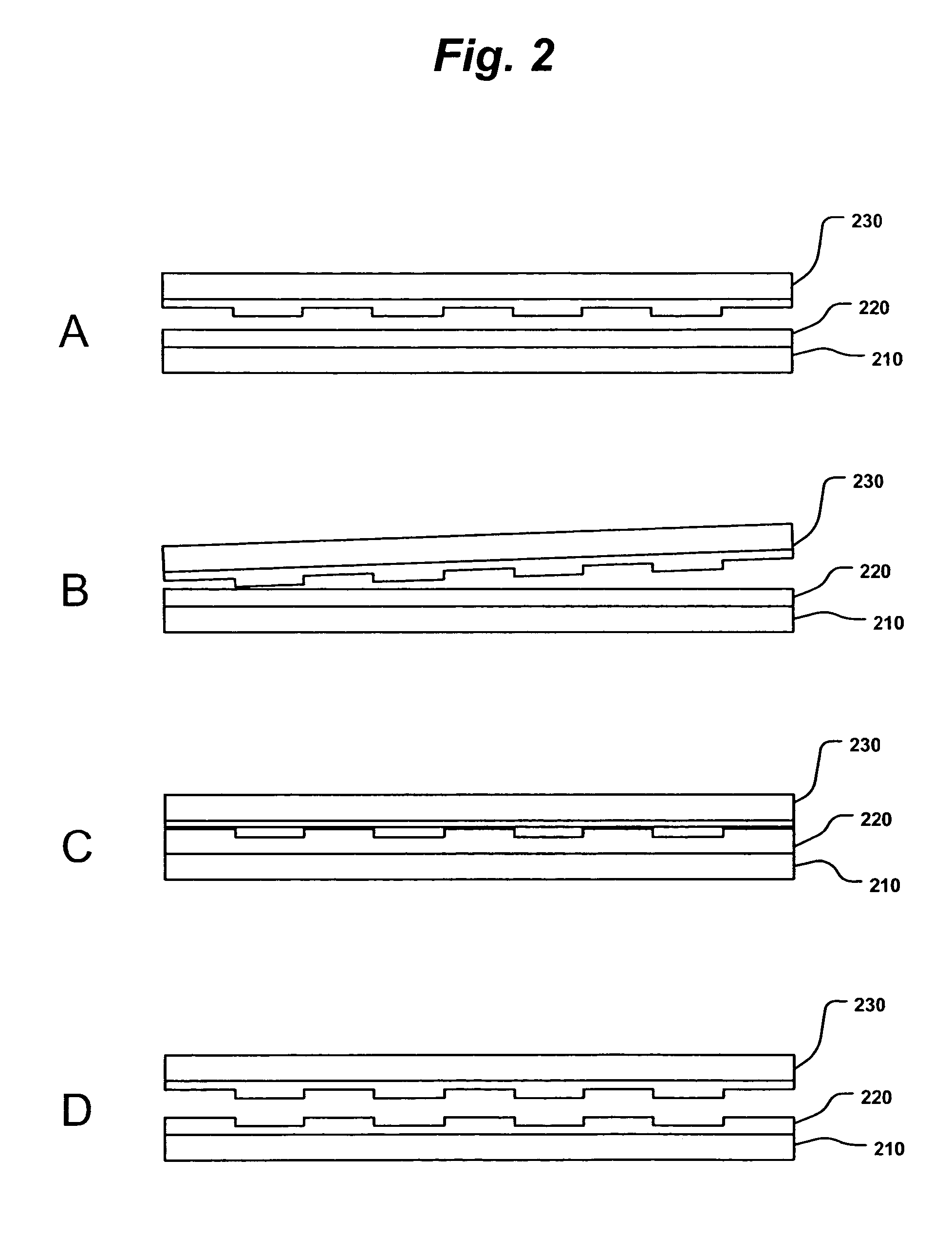
[0015] It is to be understood that the figures and descriptions of the present invention have been simplified to illustrate elements that are relevant for a clear understanding of the present invention, while eliminating, for the purpose of clarity, many other elements found in typical lithographic processes and methods of manufacturing the same. Those of ordinary skill in the art may recognize that other elements and / or steps are desirable and / or required in implementing the present invention. However, because such elements and steps are well known in the art, and because they do not facilitate a better understanding of the present invention, a discussion of such elements and steps is not provided herein.

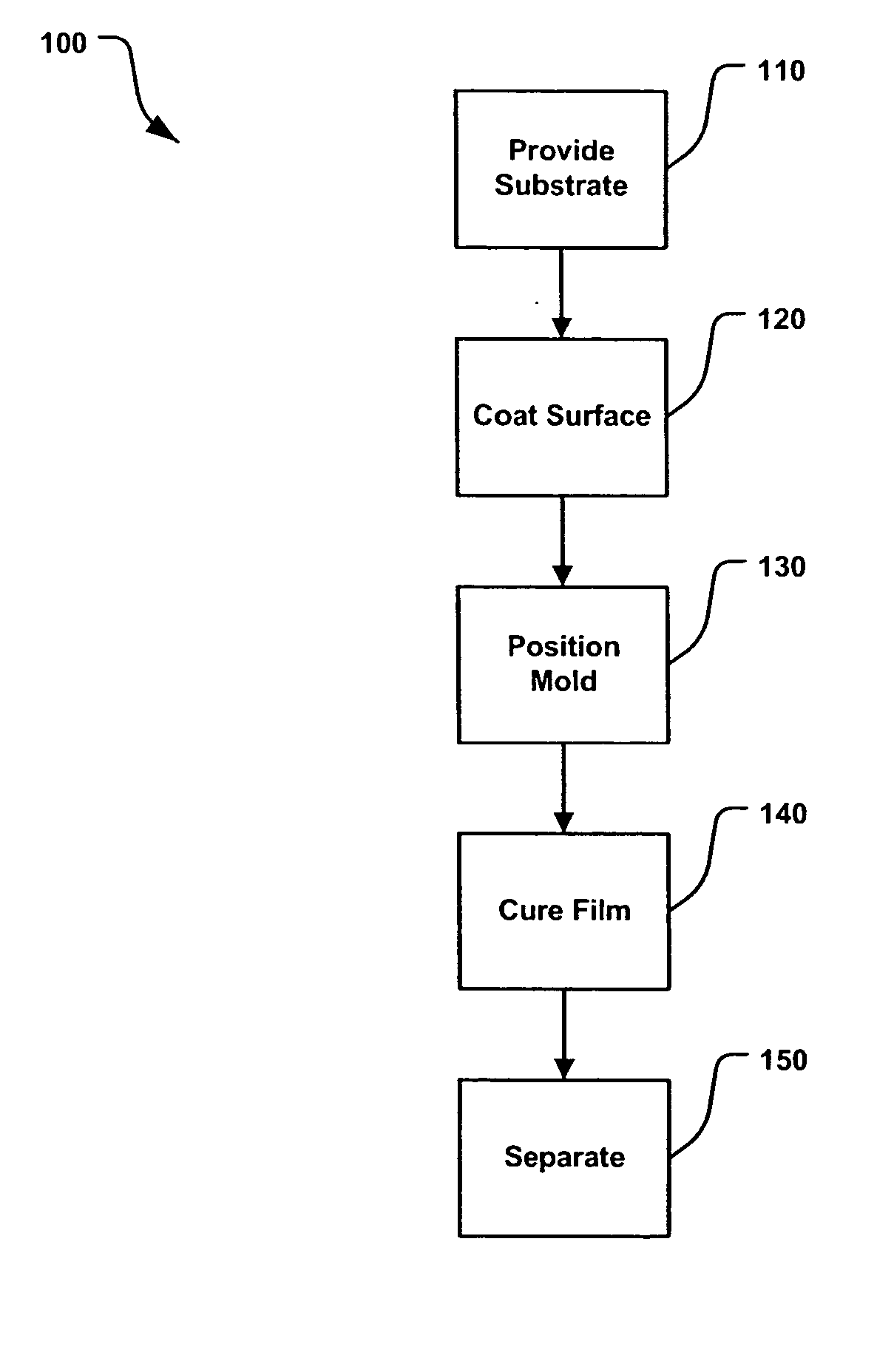
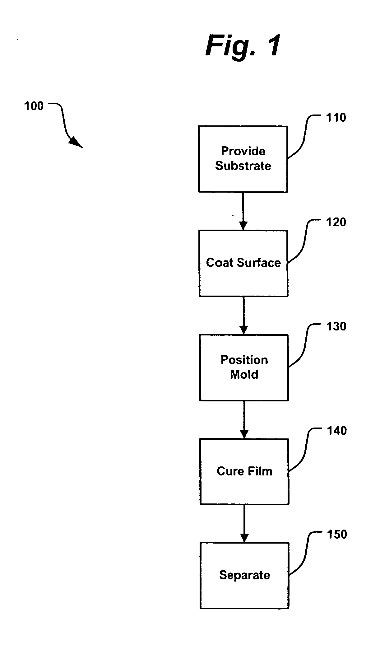
[0016] Referring now to FIG. 1, there is shown a method 100 for forming a pattern according to an aspect of the present invention. A pattern formed according to the present invention may be used as a lithography mask. Further, a pattern formed according to the present invention ma...


PUM

PropertyMeasurementUnit
diameteraaaaaaaaaa
diameteraaaaaaaaaa
diameteraaaaaaaaaa

Abstract

A method for replicating a nanopattern is disclosed. This method includes identifying a substrate; coating a surface of the substrate with a liquid layer; positioning a mold having a plurality of recesses defining a negative of the nanopattern in sufficient proximity with the coated liquid layer to cause the liquid layer to self-fill at least a portion of the plurality of recesses of the mold; and, chemically transforming the liquid layer to enable the transformed film to substantially retain the nanopattern.

Description

[0001] This application claims priority of U.S. Patent Application Ser. No. 60 / 496,193, entitled SUB-MICRON-SCALE PATTERNING METHOD AND SYSTEM, filed Aug. 19, 2003, the entire disclosure of which is hereby incorporated by reference as if being set forth in its entirety herein.FIELD OF THE INVENTION BACKGROUND OF THE INVENTION [0002] In fabricating semiconductor integrated electrical circuits, integrated optical, magnetic and mechanical circuits, and other similarly produced devices, one method of production involves molding technology, such as embossing or nanoimprinting, step and flash imprint, and mold assisted nanolithography. While each of these methods differs in the specific method and steps, or physical principle, the methods all suffer from drawbacks in forming nano-scale patterns. Each may be generally classified as including lithography. [0003] Embossing involves pressing a stamp into a polymer heated just above its transition temperature. While embossing generally produce...

Claims


Application Information

Patent Timeline
Patent Type & Authority Applications(United States)
IPC IPC(8): B05D1/32B05D3/00B29C39/10C25DG03F7/00G03F7/16H01L51/00H01L51/56
CPCB82Y10/00B82Y40/00H01L2251/105H01L51/0014H01L51/56G03F7/0002H10K71/20H10K71/821H10K71/00
Inventor WANG, JIANCHEN, LEILEE, HOWARD
Owner WANG JIAN
Why Eureka
Try Eureka