Photovoltaic device
a photovoltaic element and photovoltaic technology, applied in the direction of basic electric elements, semiconductor devices, electrical equipment, etc., can solve the problems of insufficient electric power generation efficiency, inability to use photovoltaic elements as thin film solar batteries,
- Summary
- Abstract
- Description
- Claims
- Application Information
AI Technical Summary
Benefits of technology
Problems solved by technology
Method used
Image

Examples
examples
[0060] This invention will be concretely described on the examples.
examples 1-3
[0061] In these examples, the first photovoltaic element as illustrated in FIG. 4 was fabricated. As a substrate was employed a PEN film with a thickness of 75 μm, which was set in a DC magnetron sputtering apparatus. Then, a ZnO film was formed as the first transparent electrode layer in a thickness of 70 nm. The sputtering was performed under the condition that a ZnO target was employed, and the Ar gas pressured was set to 0.5 Pa, and the input electric power was set to 2.0 W / cm2.
[0062] Then, Ni films were formed as intermediate layers in thicknesses of 2, 5, 10 nm by the same DC magnetron sputtering apparatus. The sputtering was performed under the condition that a Ni-target was employed, and the Ar gas pressure was set to 0.5 Pa, and the input electric power was set to 0.5 W / cm2.
[0063] Then, an electric power generating layer is formed by means of plasma CVD. The PEN film with the ZnO film and the Ni film was set into the plasma CVD apparatus, and heated to 160° C. Then, a B2H...
examples 4-6
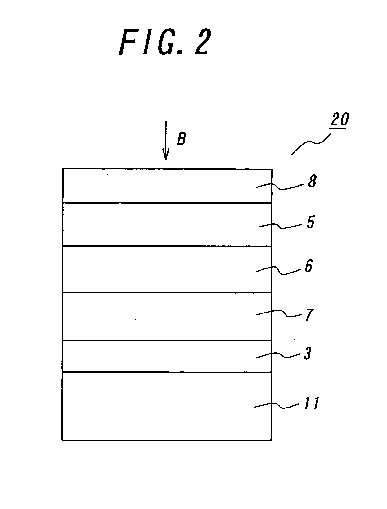
[0070] In these examples, the third photovoltaic element as illustrated in FIG. 6 was fabricated. As a substrate was employed a PEN film with a thickness of 75 μm, which was set in a DC magnetron sputtering apparatus. Then, an Al film was formed as the second substrate in a thickness of 300 nm. The sputtering was performed under the condition that an Al target was employed, and the Ar gas pressure was set to 0.5 Pa, and the input electric power was 2.2 W / cm2. Then, an ZnO film was formed as the first transparent electrode layer in a thickness of 90 nm. The sputtering was performed under the condition that a ZnO target was employed, and the Ar gas pressured was set to 0.5 Pa, and the input electric power was set to 2.0 W / cm2.
[0071] Then, Ni films were formed as intermediate layers in thicknesses of 2, 5, 10 nm by the same DC magnetron sputtering apparatus. The sputtering was performed under the condition that a Ni-target was employed, and the Ar gas pressure was set to 0.5 Pa, and t...
PUM
 Abstract
Description
Claims
Application Information
 - R&D
- Intellectual Property
- Life Sciences
- Materials
- Tech Scout
- Unparalleled Data Quality
- Higher Quality Content
- 60% Fewer Hallucinations
Browse by: Latest US Patents, China's latest patents, Technical Efficacy Thesaurus, Application Domain, Technology Topic, Popular Technical Reports.
© 2025 PatSnap. All rights reserved.Legal|Privacy policy|Modern Slavery Act Transparency Statement|Sitemap|About US| Contact US: help@patsnap.com