Bridge-type magnetic random access memory (MRAM) latch

a random access memory and latch technology, applied in the field of memory technology, can solve the problems of periodic refresh cycles, loss of data encountered, loss of data, etc., and achieve the effects of small resistance difference, reliable detection of logic states, and less manufacturing cos

Inactive Publication Date: 2005-04-28
MICRON TECH INC
View PDF30 Cites 5 Cited by
  • Summary
  • Abstract
  • Description
  • Claims
  • Application Information

AI Technical Summary

Benefits of technology

[0010] The invention relates to techniques to read a stored state in a magnetoresistive random access memory (MRAM) memory device. Advantageously, an interface circuit or latching circuit according to an embodiment of the invention is relatively insensitive to transistor parameter variations, such as gate length. This advantageously allows the interface circuit to be manufactured less expensively and also allows the interface circuit to reliably detect logic states with relatively small differences in resistance.
[0011] A bit line in an MRAM device is segmented into a first portion and a second portion. An interface circuit compares the resistance associated with a first portion and a second portion of a first bit line to the resistance associated with a first portion and a second portion of a second bit line to determine the logical state of a cell in the first bit line. The interface circuit includes a reset circuit to allow the circuit to achieve a balanced state by coupling outputs of the interface circuit to a relatively low resistance. Decoupling of the outputs allows cross-coupling within the interface circuit to latch the outputs to a logical state corresponding to the stored magnetic state, thereby allowing the stored state of a cell to be read.

Problems solved by technology

A volatile memory loses its data when power is removed.
In addition, certain volatile memories, such as DRAM devices, require periodic refresh cycles to retain their data even when power is continuously supplied.
In contrast to the potential loss of data encountered in volatile memory devices, nonvolatile memory devices retain data for long periods of time when power is removed.
Disadvantageously, conventional nonvolatile memories are relatively large, slow, and expensive.
Further, many types of conventional semiconductor nonvolatile memories are relatively limited in write cycle capability and typically can only be programmed to store data about 10,000 times in a particular memory location.
Disadvantageously, conventional circuits that latch the state of the magnetic memory cell are relatively sensitive to variations in transistor parameters, such as gate length.
These sensitivities can disadvantageously increase production costs and can also cause data to be incorrectly read from the magnetic memory cell.

Method used


Image

  • Bridge-type magnetic random access memory (MRAM) latch
  • Bridge-type magnetic random access memory (MRAM) latch
  • Bridge-type magnetic random access memory (MRAM) latch

Examples


Embodiment Construction

[0025] Although this invention will be described in terms of certain preferred embodiments, other embodiments that are apparent to those of ordinary skill in the art, including embodiments that do not provide all of the benefits and features set forth herein, are also within the scope of this invention. Accordingly, the scope of the invention is defined only by reference to the appended claims.

[0026] A magnetoresistive random access memory (MRAM) stores data in magnetic states of its memory cells. The electrical resistance of the cell varies depending on the stored magnetic state of the cell. The stored state of the cell is detected by sensing the difference in resistance.

[0027] While illustrated in the context of giant magneto-resistance (GMR) memories, the skilled artisan will appreciate that the principles and advantages described herein are applicable to other types of magnetic memories, such as tunneling magneto-resistance (TMR) MRAMs.

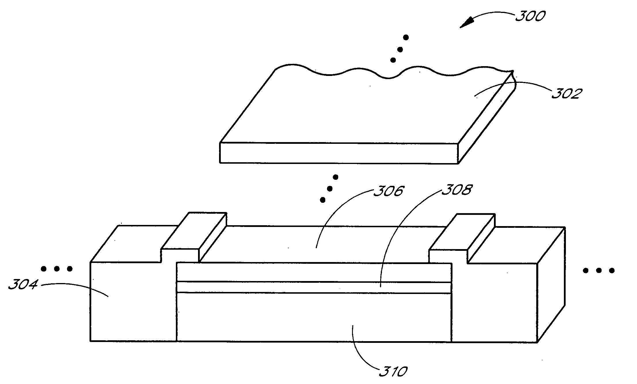
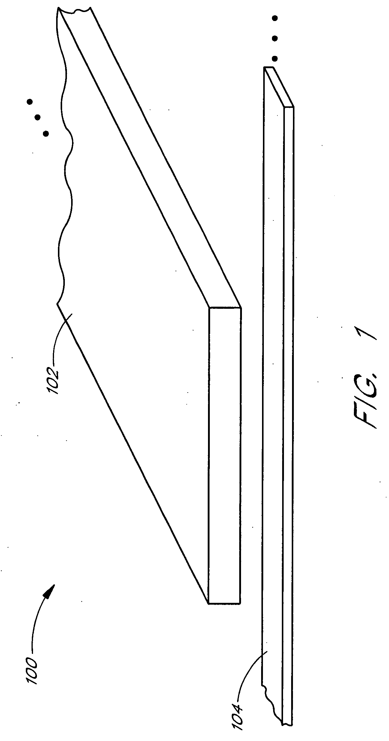
[0028]FIG. 1 is a perspective view illus...


PUM


Abstract

A technique to read a stored state in a magnetoresistive random access memory (MRAM) device, such as a giant magneto-resistance (GMR) MRAM device or a tunneling magneto-resistance (TMR) device uses a bit line in an MRAM device that is segmented into a first portion and a second portion. An interface circuit compares the resistance of a first portion and a second portion of a first bit line to the resistance of a first portion and a second portion of a second bit line to determine the logical state of a cell in the first bit line. The interface circuit includes a reset circuit that selectively couples the outputs of the interface circuit together. A subsequent decoupling of the outputs allows cross-coupling within the interface circuit to latch the outputs to a logical state corresponding to the stored magnetic state, thereby allowing the stored state of a cell to be read.

Description

RELATED APPLICATION [0001] This application is a continuation application of U.S. application Ser. No. 10 / 775,582, filed on Feb. 10, 2004, which is a continuation of U.S. application Ser. No. 10 / 246,245, filed Sep. 17, 2002, now U.S. Pat. No. 6,714,441, issued on Mar. 30, 2004, the disclosures of which are hereby incorporated by reference in their entirety herein.GOVERNMENT RIGHTS [0002] This invention was made with Government support under Contract Number MDA972-98-C-0021 awarded by DARPA. The Government has certain rights in the invention.BACKGROUND OF THE INVENTION [0003] 1. Field of the Invention [0004] The invention generally relates to memory technology. In particular, the invention relates to non-volatile magnetic memory. [0005] 2. Description of the Related Art [0006] Computers and other digital systems use memory to store programs and data. A common form of memory is random access memory (RAM). Many memory devices, such as dynamic random access memory (DRAM) devices and sta...

Claims


Application Information

Patent Timeline
Patent Type & Authority Applications(United States)
IPC IPC(8): G11C11/15
CPCG11C11/15
Inventor FULKERSON, DAVID E.LU, YONG
Owner MICRON TECH INC
Why Eureka
Try Eureka