Wafer dividing method

Active Publication Date: 2005-04-28
DISCO CORP
View PDF3 Cites 34 Cited by
  • Summary
  • Abstract
  • Description
  • Claims
  • Application Information

AI Technical Summary

Benefits of technology

[0006] It is an object of the present invention to provide a method of dividing a wafer, comprising applying a laser beam to a wafer a

Problems solved by technology

However, the above dividing method has a problem with productivity because the wafer cannot be divided along the dividing lines simply by forming the deteriorated layers in the i

Method used


Image

  • Wafer dividing method
  • Wafer dividing method
  • Wafer dividing method

Examples


experimental example 1

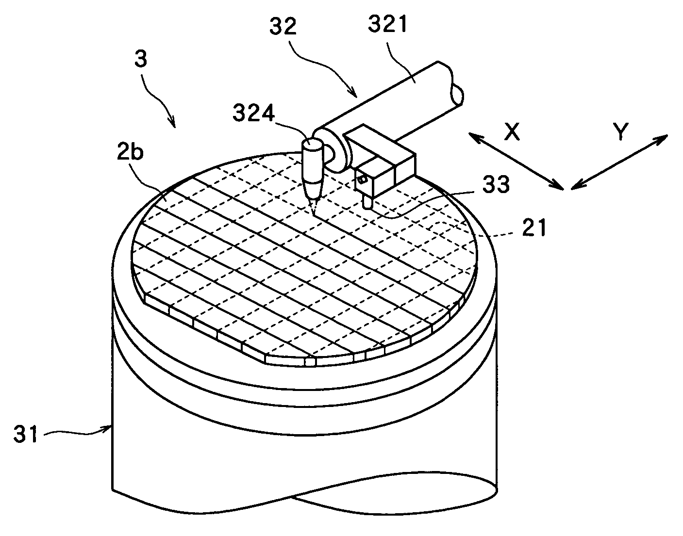
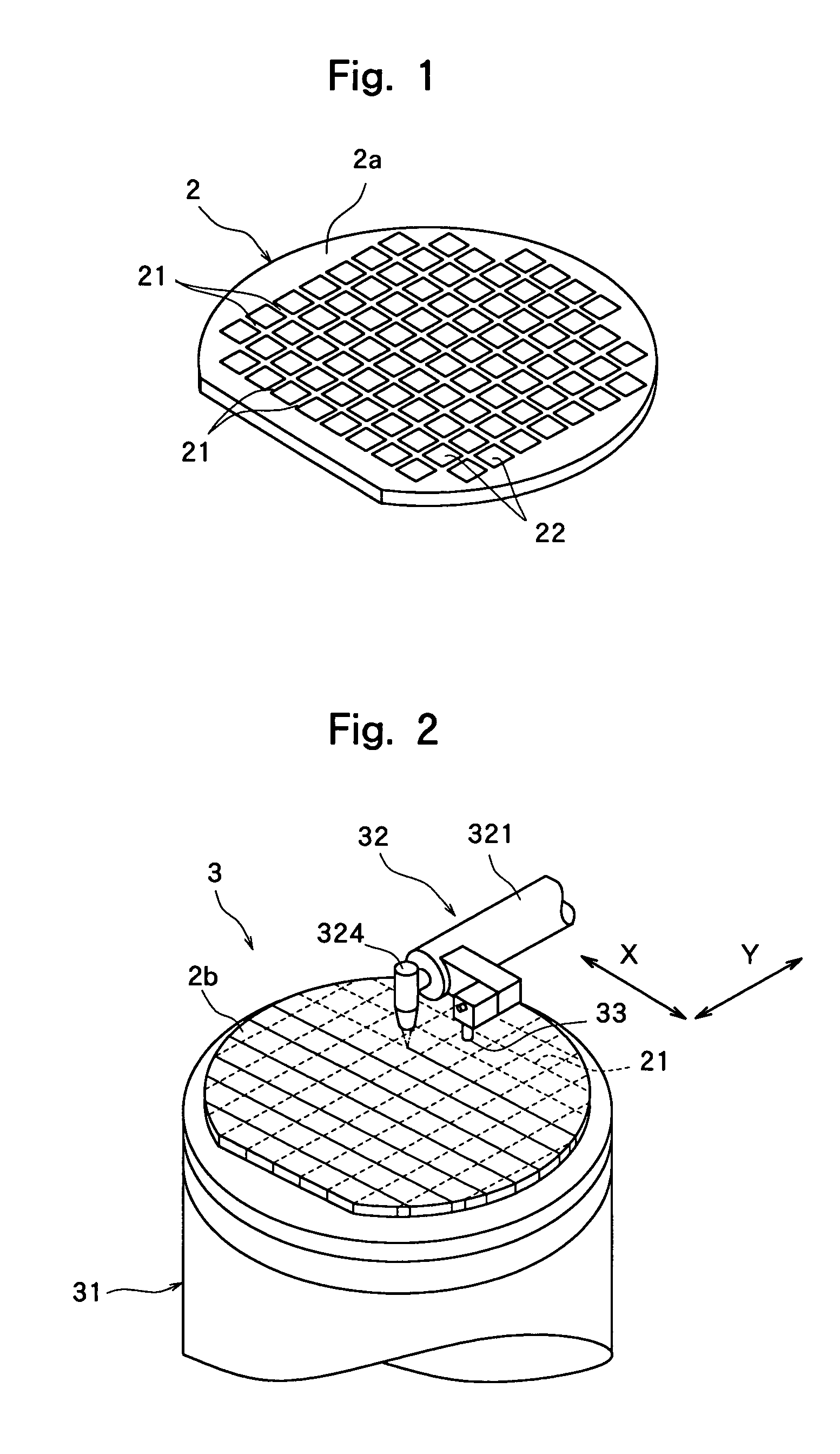
[0051] The above deteriorated layers were formed in a semiconductor wafer having a diameter of 6 inches and a thickness of 300 μm by changing the above coefficient k in a range of from 0.1 to 4.0 under the above processing conditions, and stress required for dividing the semiconductor wafer along each dividing line was measured in each of cases. For the measurement of stress, a three-point bending test was carried out in which the back surface of the semiconductor wafer was supported along the dividing line at positions 2.0 mm away from the dividing line on both sides and a load was applied to the front surface of the semiconductor wafer along the dividing line. The measured stress was stress on a cross section based on the load at the time when the semiconductor wafer was divided. The measurement results are shown in FIG. 10. It is understood that when the coefficient k is 1.0 to 2.5, stress required for dividing the semiconductor wafer is small.

[0052] After the deteriorated layer...

experimental example 2

[0056] A semiconductor wafer (silicon wafer) having a diameter of 6 inches and a thickness of 300 μm was divided into semiconductor chips of 2 mm×2 mm by the above-described method. FIG. 15 shows the yield rate of semiconductor chips obtained by dividing the semiconductor wafer along the deteriorated layers by carrying out the above dividing step (to be referred to as “tape expanding method” hereinafter) when the repetition frequency of the pulse laser beam applied in the above deteriorated layer forming step was set to 100 kHz, 150 kHz, 200 kHz, 300 kHz or 400 kHz (in this Example, the above coefficient k was 1). In FIG. 15, the horizontal axis shows the repetition frequency of the pulse laser beam applied in the above deteriorated layer forming step and the vertical axis shows the chip yield rate obtained by dividing the number of semiconductor chips obtained from the semiconductor wafer by carrying out the above tape expanding method, by the number of semiconductor chips formed o...


PUM

PropertyMeasurementUnit
Electric potential / voltageaaaaaaaaaa
Frequencyaaaaaaaaaa

Abstract

A method of dividing a wafer along predetermined dividing lines, comprising the steps of a deteriorated layer forming step for applying a pulse laser beam capable of passing through the wafer along the dividing lines to form deteriorated layers in the inside of the wafer along the dividing lines; an extensible protective tape affixing step for affixing an extensible protective tape to one side of the wafer before or after the deteriorated layer forming step; and a dividing step for dividing the wafer along the deteriorated layers by expanding the protective tape affixed to the wafer after the deteriorated layer forming step.

Description

FIELD OF THE INVENTION [0001] The present invention relates to a method of dividing a wafer having dividing lines formed on the front surface thereof along the dividing lines. DESCRIPTION OF THE PRIOR ART [0002] In the production process of a semiconductor device, a large number of rectangular areas are sectioned by dividing lines called “streets” arranged in a lattice pattern on the front surface of a substantially disk-like semiconductor wafer such as a silicon wafer, and a circuit such as IC or LSI is formed in each of the rectangular areas. Individual semiconductor chips are manufactured by dividing this semiconductor wafer having a large number of circuits formed thereon along the dividing lines. The semiconductor chips are widely used in electric equipment such as mobile telephones, personal computers, etc. Dividing along the dividing lines is generally carried out by a cutting machine called “dicer”. This cutting machine comprises a chuck table for holding a plate-like workpi...

Claims


Application Information

Patent Timeline
IPC IPC(8): B23K26/38B23K26/40B23K101/40B28D5/00H01L21/301H01L21/304H01L21/78
CPCB23K26/0057B23K26/4075H01L21/78H01L21/3043B28D5/0011B23K26/40B23K26/53B23K2103/50
Inventor NAGAI, YUSUKENAKAMURA, MASURUKOBAYASHI, SATOSHIMORISHIGE, YUKIO
Owner DISCO CORP
Why Eureka
Try Eureka