Method of dividing wafer

a technology of dividing wafers and wafers, applied in the direction of electrical equipment, semiconductor devices, semiconductor/solid-state device details, etc., can solve the problems of complex whole-wafer processing sequence and high cost, and achieve the effect of reducing cost, facilitating removal, and efficiently dividing wafers into individual chips

a technology of dividing wafers and wafers, applied in the direction of electrical equipment, semiconductor devices, semiconductor/solid-state device details, etc., can solve the problems of complex whole-wafer processing sequence and high cost, and achieve the effect of reducing cost, facilitating removal, and efficiently dividing wafers into individual chips

US20160307851A1Inactive Publication Date: 2016-10-20DISCO CORP

Image

  • Method of dividing wafer
  • Method of dividing wafer
  • Method of dividing wafer

Examples


Embodiment Construction

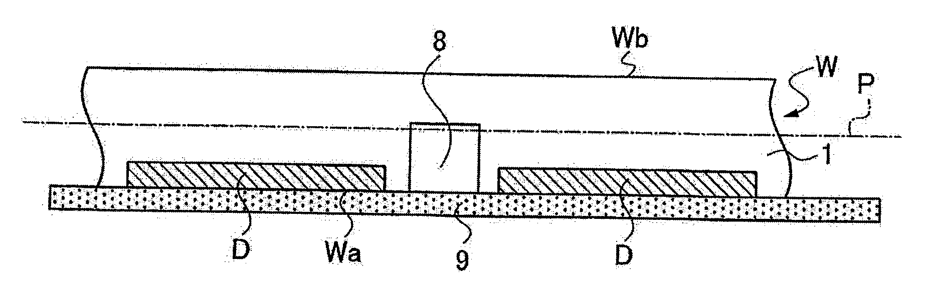
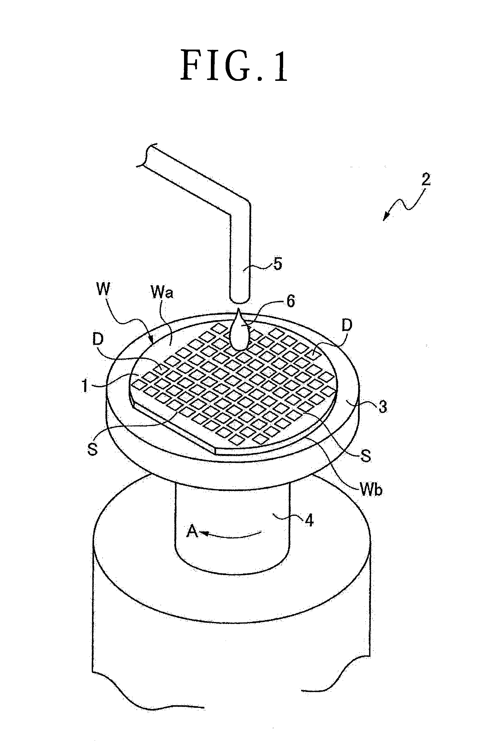
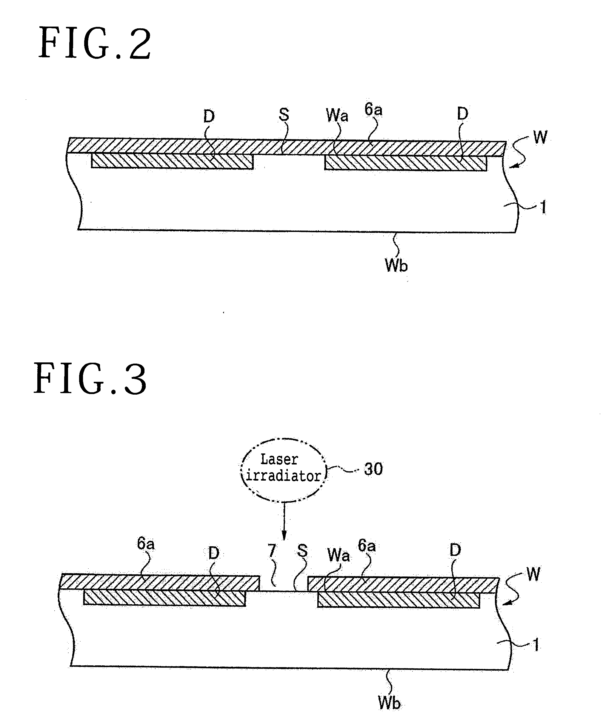
[0025]A wafer W depicted in FIG. 1, which represents an example of a workpiece to be processed, has a substrate 1 in the shape of a circular plate. The wafer W has a plurality of streets S formed on a front side Wa thereof and devices D formed in respective areas defined by the streets S. A face of the wafer W which is opposite to the front side Wa is referred to as a back side Wb to be grounded by grinding stones or the like. A method of dividing the wafer W into the individual devices D will be described below.

(1) Protective Film Forming Step

[0026]As depicted in FIG. 1, a water-soluble protective film is formed on the front side Wa of the wafer W using a spin coater 2, for example. The spin coater 2 has a rotatable spinner table 3 that holds the wafer W thereon. A rotational shaft 4 having a vertical axis is connected to the lower side of the spinner table 3. A nozzle 5 for ejecting a material liquid for the water-soluble protective film is disposed above the spinner table 3, and ...


PUM


Abstract

A method of dividing a wafer includes a protective film forming step of forming a water-soluble protective film on a front side of the wafer, a mask forming step of forming an etching mask on the front side of the wafer by partly removing the water-soluble protective film along the streets, a plasma etching step of performing a plasma etching on the wafer along the streets through the etching mask in the form of the water-soluble protective film, and a protective film removing step of removing the water-soluble protective film by supplying cleaning water to the water-soluble protective film. After plasma etching, i.e. in removing the protective film, the water-soluble protective film can easily be removed from the front side of the wafer simply by supplying the cleaning water from a water supply unit to the water-soluble protective film.

Description

BACKGROUND OF THE INVENTION[0001]1. Field of the Invention[0002]The present invention relates to a method of dividing a wafer into individual chips.[0003]2. Description of the Related Art[0004]In the process of fabricating devices, a plurality of chip areas are defined on the front side of a wafer by a plurality of division lines arranged in a grid pattern on the front side of the wafer, and devices such as ICs, LSI circuits, etc. are formed in the respective chip areas. The wafer thus arranged is reduced to a predetermined thickness by having its back side ground, and then is divided into chips provided with individual devices, after which the chips are resin-sealed into packages that will be widely used in various electronic instruments including cellular phones, personal computers, etc.[0005]For dividing a wafer, there have been proposed a method of cutting the wafer along division lines with a cutting blade that is rotated and displaced to incise the wafer and a method of applyi...

Claims


Application Information

Patent Timeline
20 Oct 2016
Publication
US20160307851A1
IPC
H01L23/544; H01L21/683; H01L21/78
CPC
H01L23/544; H01L21/78; H01L2223/5446; H01L2221/68327; H01L2221/6834; H01L21/6836; H01L21/30655; H01L21/3081
Inventors
OHURA, YUKINOBU; YAMASHITA, YOHEI