Semiconductor device and wire bonding method

a technology of semiconductor devices and wire bonds, which is applied in the direction of metal working equipment, non-electric welding equipment, manufacturing tools, etc., can solve the problems of cracks, cracks, etc., and rise of wires, so as to achieve the effect of not damage to pads

Inactive Publication Date: 2005-05-05
SHINKAWA CO LTD
View PDF18 Cites 18 Cited by
  • Summary
  • Abstract
  • Description
  • Claims
  • Application Information

AI Technical Summary

Benefits of technology

[0008] The object of the present invention is to provide a semiconductor device and a wire bonding method that ...

Problems solved by technology

However, in ball bonding, a rise occurs in the wire; as a result, the looped wire tends to be high when the primary bonding is performed on the pad of the die.
However, in wedge bonding that constitutes secondary bonding, the wire itself is bonded, and the wire is cut; accordingly, the und...

Method used


Image

  • Semiconductor device and wire bonding method
  • Semiconductor device and wire bonding method
  • Semiconductor device and wire bonding method

Examples


Embodiment Construction

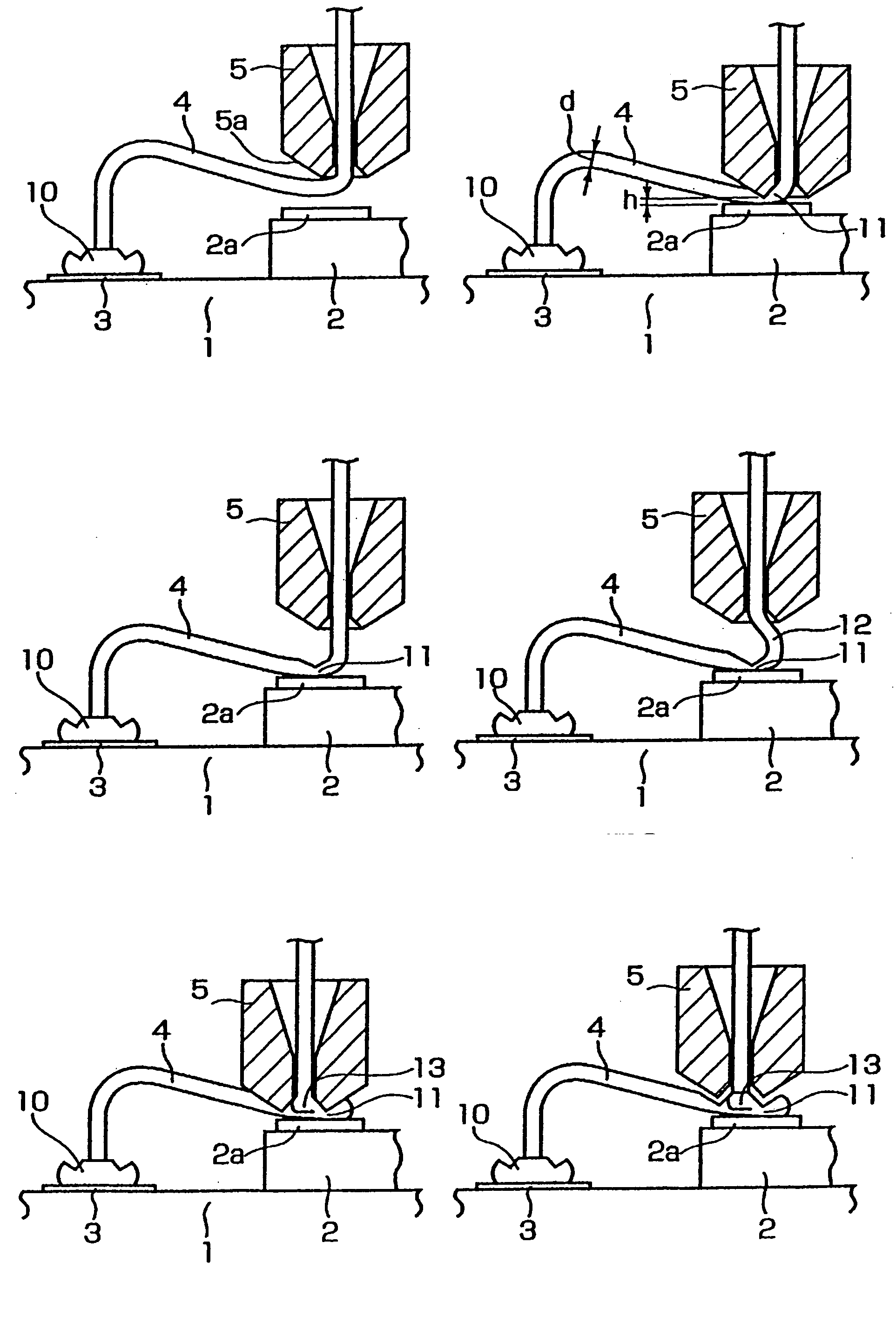
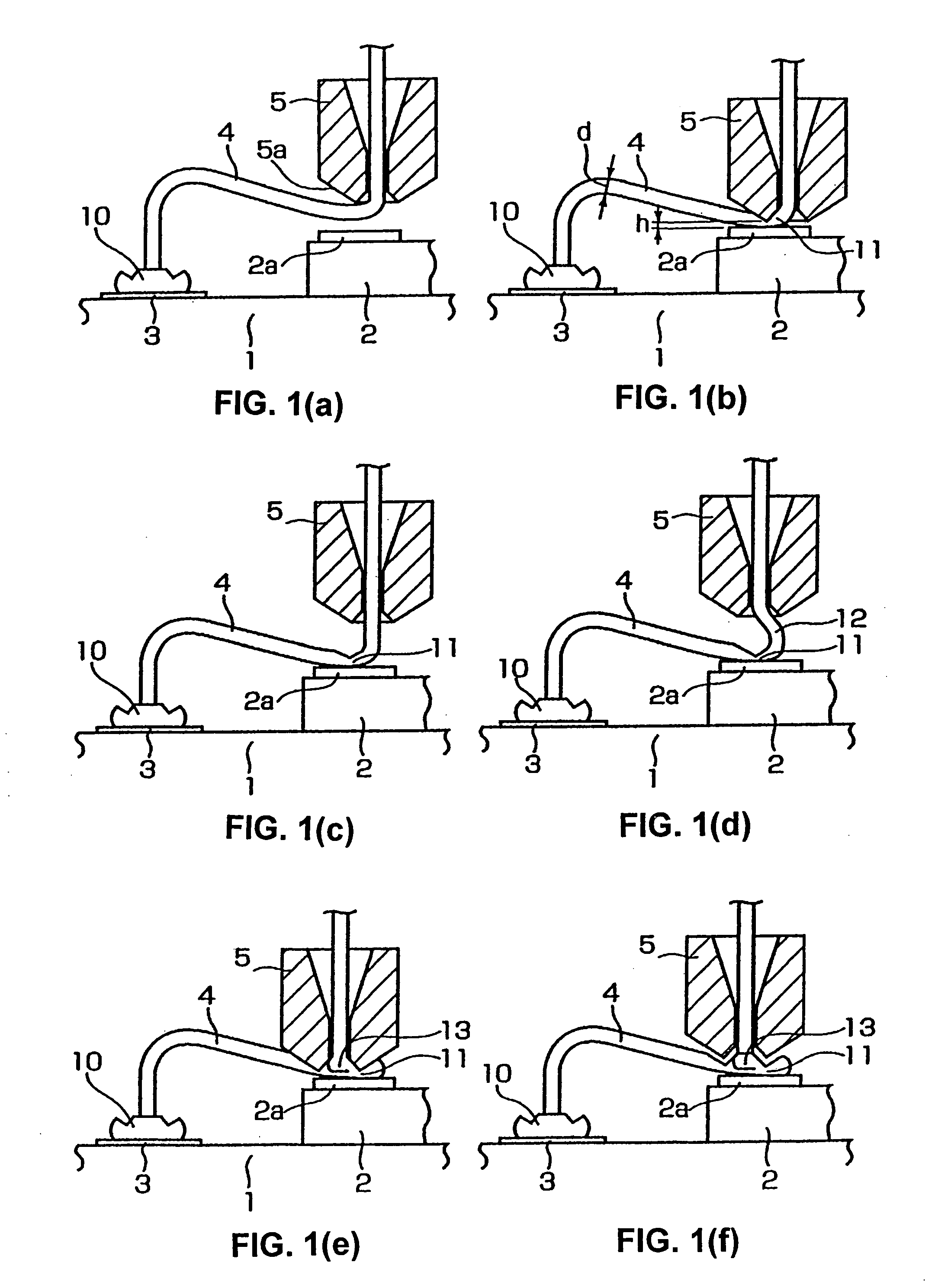
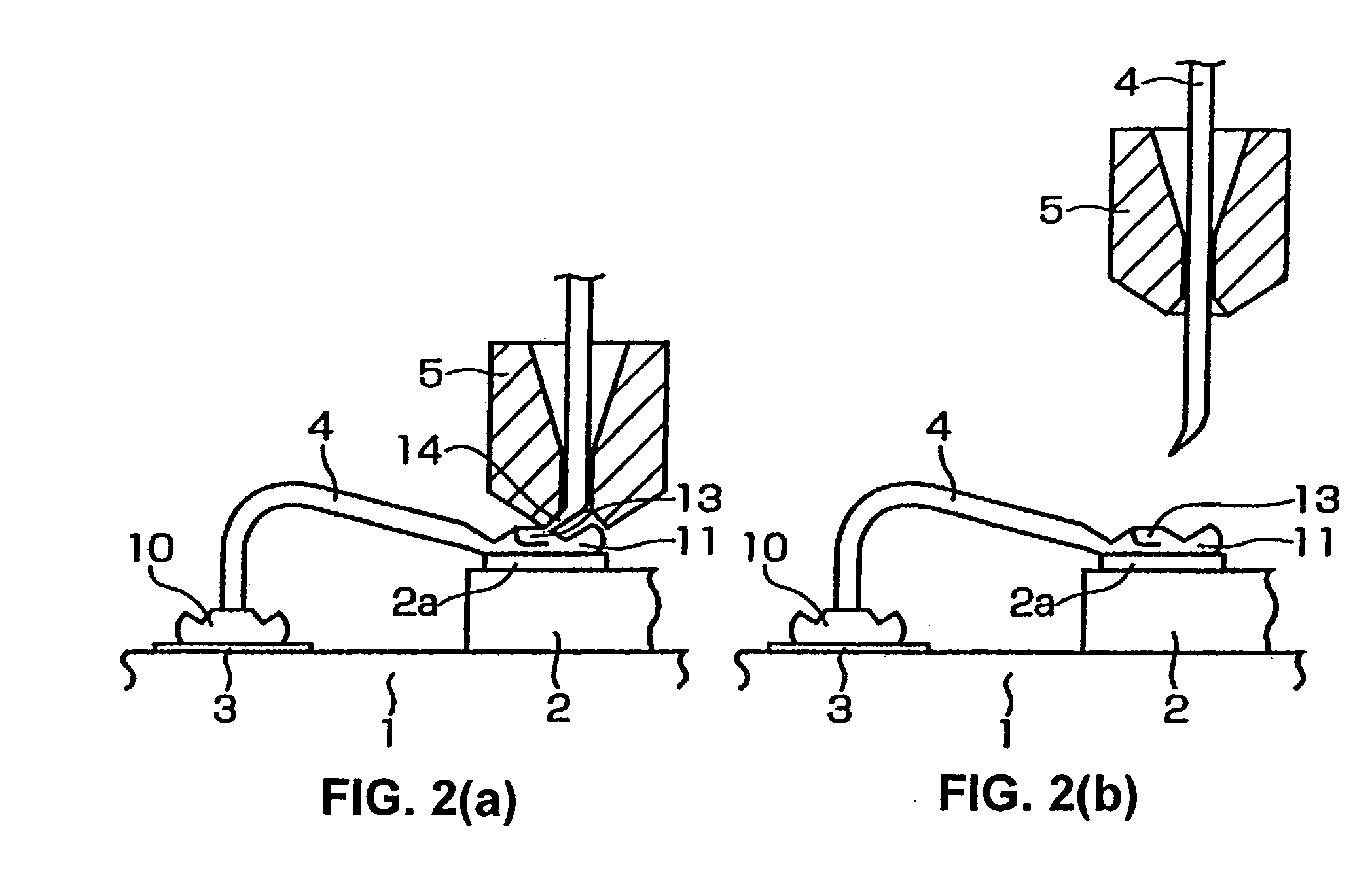
[0021] One embodiment of the semiconductor device of the present invention will be described with reference to FIG. 2(b) that shows a completed semiconductor.

[0022] A die 2 on which a pad 2a is formed is mounted on a circuit board 1, which is a ceramic board, a printed board, a lead frame, etc. Wiring 3 is formed on the circuit board 1.

[0023] In this semiconductor device, a ball formed on the tip end of a wire 4 is connected to the wiring 3 that is the first bonding point, thus forming a crimped ball 10; and the wire 4 is connected to a pad 2a which is on the die 2, the pad 2a being the second bonding point, so that the wiring 3 and pad 2a are connected by the wire 4. The connected shape of the wire on the pad 2a that constitutes the second bonding point is comprised of a first bonding part 11 formed by the connection of the wire 4 to the pad 2a and a second bonding part 13 formed by overlapping and connecting the wire 4 to this first bonding part 11.

[0024] Thus, the connection o...


PUM


Abstract

A wire bonding method that performs a primary bonding of wire on a first bonding point and performs a secondary bonding of the wire on a second bonding point, thus connecting the first and second bonding points with the wire, the secondary bonding including: a first bonding step that forms a first bonding part by bonding the wire to the second bonding point, a second bonding step that forms a second bonding part by raising a capillary through which the wire passes and moving the capillary toward the first bonding point, and then lowering the capillary and overlapping the wire to connect the wire to the first bonding part, and a ting step that cuts the wire.

Description

BACKGROUND OF THE INVENTION [0001] 1. Technical Field [0002] The present invention relates to a semiconductor device and wire bonding method in which a pad on a die and wiring of a circuit board are connected by a wire. [0003] 2. Description of the Related Art [0004] A die on which pads are formed is mounted on a circuit board on which wiring is formed. The connection of a wire between such pads and wiring is, in order to prevent damages to the pad, generally accomplished by performing ball bonding (a primary bonding) on the pad of a die, looping the wire, and then performing wedge bonding (a secondary bonding) on the wiring. However, in ball bonding, a rise occurs in the wire; as a result, the looped wire tends to be high when the primary bonding is performed on the pad of the die. [0005] Accordingly, in one method, primary bonding is performed on the wiring, and secondary bonding is performed on the pad of the die, thus being a reverse of that described above. However, in wedge bo...

Claims


Application Information

Patent Timeline
IPC IPC(8): H01L21/60B23K20/00H01L21/607
CPCB23K20/005H01L2224/4809H01L24/48H01L24/78H01L24/85H01L2224/05599H01L2224/48091H01L2224/48225H01L2224/48471H01L2224/78301H01L2224/8518H01L2224/85186H01L2224/85205H01L2224/85399H01L2224/85951H01L2924/01004H01L2924/01005H01L2924/01006H01L2924/01082B23K2201/40H01L2924/01033H01L2924/00014H01L2224/45099H01L2924/00B23K2101/40H01L2224/48227H01L2924/15787
Inventor MII, TATSUNARI
Owner SHINKAWA CO LTD
Why Eureka
Try Eureka