Mounting member of semiconductor device, mounting configuration of semiconductor device, and drive unit of semiconductor device

a technology of mounting configuration and semiconductor device, which is applied in the direction of individual semiconductor device testing, semiconductor/solid-state device testing/measurement, instruments, etc., can solve the problems of large current as the operating power supply cannot be supplied to the semiconductor device (high-power device) whose current consumption is large, and the leakage-current in a highly integrated cpu has been increasing, so as to achieve the effect of stable supply of actuating curren

Active Publication Date: 2005-05-05
ESPEC CORP
View PDF12 Cites 0 Cited by
  • Summary
  • Abstract
  • Description
  • Claims
  • Application Information

AI Technical Summary

Benefits of technology

[0012] An object of the present invention is to provide a drive unit of a semiconductor device enabling a stable supply of an actuating current to a high-power semiconductor device in which the actuating current exceeds 100 amperes.
[0015] Instead of using the wiring substrate layer of the wiring substrate, the power supplying conductor plate and the ground conductor plate respectively use thick conductor plates (for example, copper plates having a thickness of about 1 mm). Consequently, it is possible to secure a significantly larger conductor cross sectional area than a conventional one. This allows the resistance loss of the conductor to be minimized even when a large current is supplied. It is possible to swiftly follow any change in the current consumption due to any change in the operating condition, thereby stably supplying the power source.

Problems solved by technology

And, a leakage-current in a highly integrated CPU has been increasing due to the deterioration in insulation caused by miniaturization of circuit patterns or the like.
This also causes the increasing of the current consumption in the CPU.
However, in an arrangement in which the wirings and the electrode pads for the actuating power supply, GND, and signal input-output are formed on a single wiring layer of the printed circuit board, the following problem arises.
More specifically, the problem that a large current as operating power supply may not be supplied to the semiconductor device (high-power device) whose current consumption is large.
This causes the problem that the printed circuit board itself generates heat, and / or is unable to follow the change in current consumption caused by the change in the operating conditions of the semiconductor device.
This is because a conductor cross sectional area suitable for the driving current is not secured, and because a power loss increases proportionally as the square of the current value with respect to the conductor resistance.
Conventional high-power devices are not highly integrated, and they supply as power sources a current of not more than approximately 30 amperes.
However, the problem arises that a semiconductor device, which has been recently developed and consumes a large current of over 100 amperes, can not supply appropriate current even if the above conventional arrangement is adopted.
Thus, when supplying a large current of over 100 amperes to a semiconductor device, it is not possible to solve a problem such as the heat generation within the printed circuit board.
This is because the power loss increases due to the thin conductor of not more than 70 micrometers in the printed circuit board.
If it is intended to solve the problem of the current supply by making the printed circuit board to have more layers, then the cost of the printed circuit board will dramatically increase.
This results in that a drop of the voltage to be supplied to the semiconductor device due to the resistance loss of the conductor is no longer tolerated.
This gives rise to at least the following defects in the drive unit, of a burn-in apparatus, for supplying the actuating current to the semiconductor device.
Namely, a DC power supply for compensating the voltage drop becomes bulky, and a cooling device for the heat generated becomes bulky.

Method used


Image

  • Mounting member of semiconductor device, mounting configuration of semiconductor device, and drive unit of semiconductor device
  • Mounting member of semiconductor device, mounting configuration of semiconductor device, and drive unit of semiconductor device
  • Mounting member of semiconductor device, mounting configuration of semiconductor device, and drive unit of semiconductor device

Examples


Embodiment Construction

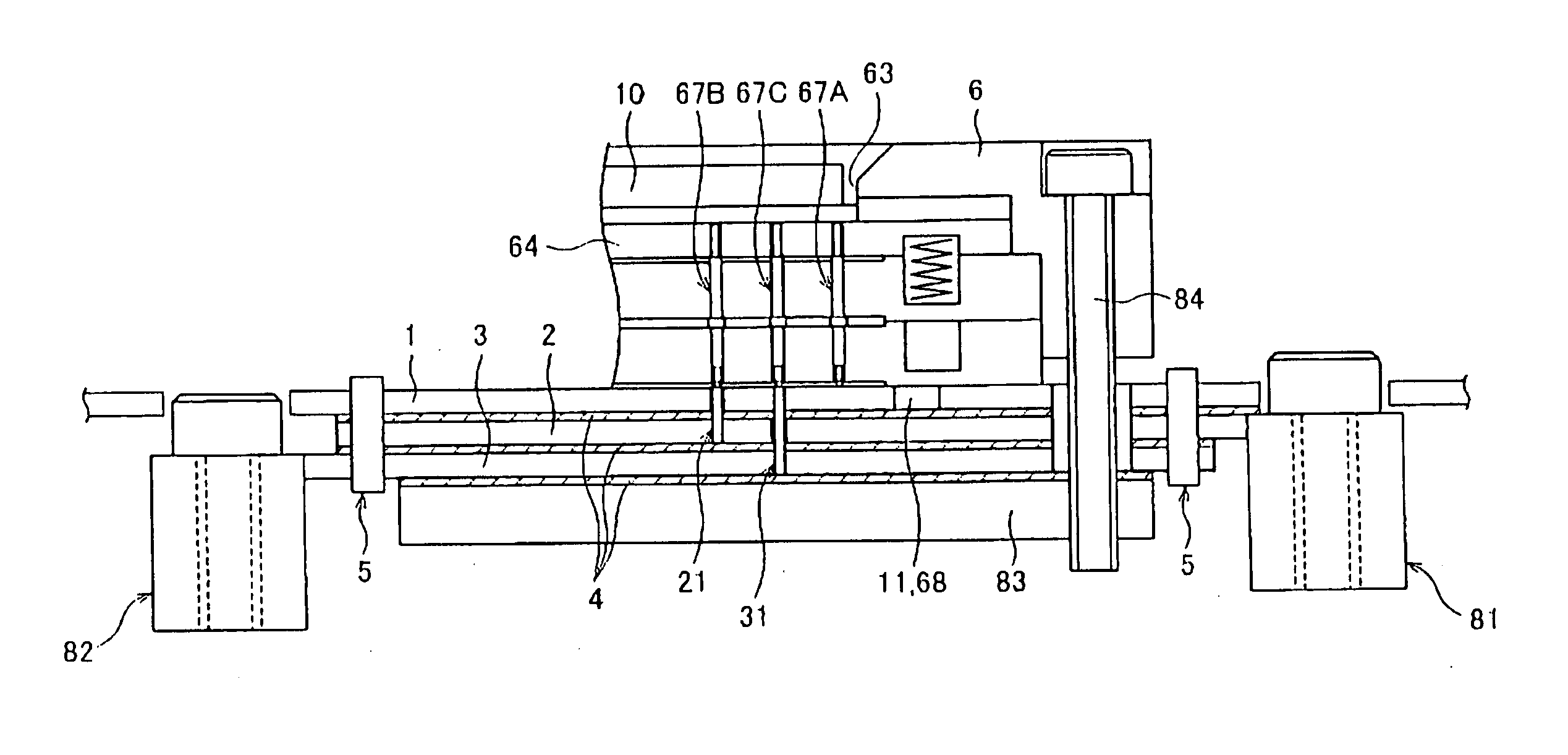
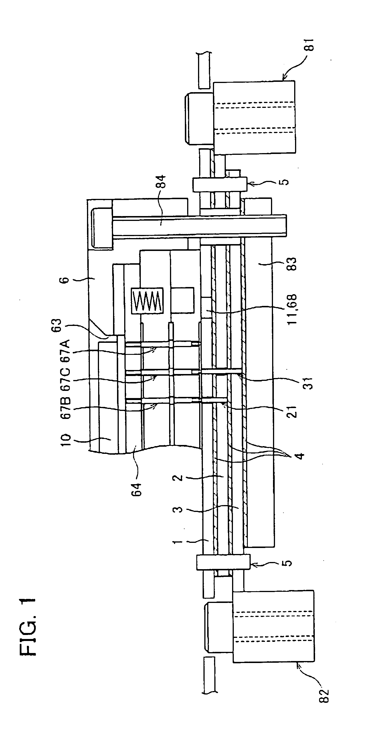
[0022] An embodiment according to the present invention is described below referring to the figures. The present embodiment deals with a case where the present invention is applied to a burn-in apparatus. Namely, note that the burn-in apparatus described below is deemed to fall within a drive unit of the semiconductor device in accordance with the present invention.

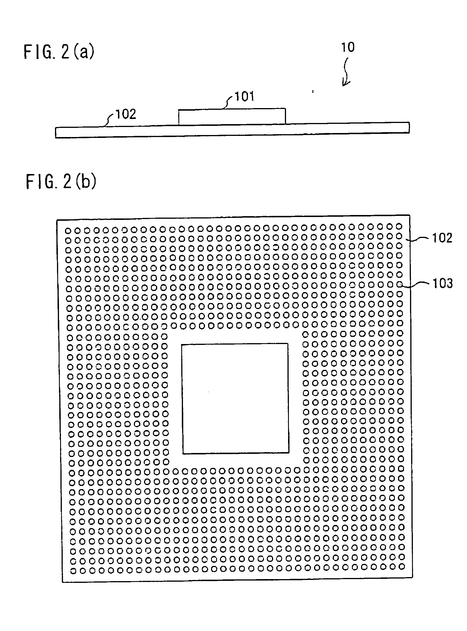
[0023] First, how the semiconductor device is arranged is described referring to FIG. 2(a) and 2(b). As shown in FIG. 2(a), a semiconductor device 10 is arranged such that a semiconductor chip 101 is mounted on a device substrate 102. A large number of electrode pads 103 are formed, in a matrix manner, on a rear surface of the device substrate 102 (on a side opposite to a side where the semiconductor chip 101 is mounted). The electrode pads 103 are connected with a printed wiring on a front side of the device substrate 102 (on the side where the semiconductor chip 101 is mounted).

[0024] Note that the entire electrode pa...


PUM


Abstract

A mounting member of a semiconductor device according to the present invention includes a wiring substrate to input and / or output actuating signals to a semiconductor device, a power supplying conductor plate to supply actuating power to the semiconductor device, and the GND conductor plate. The wiring substrate, the power supplying conductor plate, and the GND conductor plate are laminated with insulation films between respective layers. Input / output signals as well as minute driving current is supplied from wiring substrate, and the large main driving current is supplied through the power supplying conductor plate as well as the GND conductor plate.

Description

[0001] This Nonprovisional application claims priority under 35 U.S.C. § 119(a) on Patent Application No. 2003 / 373136 filed in Japan on Oct. 31, 2003, the entire contents of which are hereby incorporated by reference. FIELD OF THE INVENTION [0002] This invention is related to a drive unit of a semiconductor device in which a semiconductor chip is mounted on a substrate, and particularly to a drive unit of a semiconductor device in which a high-power semiconductor chip is mounted on a substrate, the high-power semiconductor chip whose current consumption is large. BACKGROUND OF THE INVENTION [0003] Actuating current in CPUs (Central Processing Unit) today tends to increase due to high integration caused by the growth in arithmetic capabilities. And, a leakage-current in a highly integrated CPU has been increasing due to the deterioration in insulation caused by miniaturization of circuit patterns or the like. This also causes the increasing of the current consumption in the CPU. Unde...

Claims


Application Information

Patent Timeline
Patent Type & Authority Applications(United States)
IPC IPC(8): G01R31/30H01L21/68G01R31/26H01L23/12H01L23/498H01L23/50
CPCH01L21/6835H01L23/49838H01L23/50H01L2924/0002H01L2924/00H01L23/12
Inventor OI, KENICHI
Owner ESPEC CORP
Why Eureka
Try Eureka